SBAA549 April 2022 AMC23C11 , AMC23C12 , AMC23C14
3 DC+ Power Supply Solution
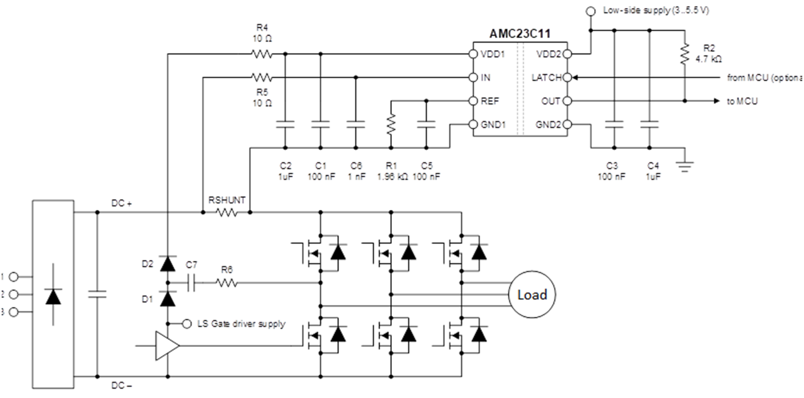
Figure 3-1 shows the implementation of a DC+ power supply.

Figure 3-1 DC+ Power Supply Solution
The DC+ power supply solution consists of two parts. The first part is a bootstrap circuit consisting of a high-voltage diode D1, a capacitor C7 and current-limiting resistor R6. C7 is charged by the low-side gate driver power supply. The second part is a charge pump consisting of a high-voltage diode D2, a capacitor C2 and current-limiting resistor R4. When the half bridge starts to operate there are three operating states as follows:
- When the low-side IGBT turns on, C7 is charged by the power supply of the low-side gate driver and D2 is turned off.
- When the high-side IGBT turns on, D2 conducts, C7 charges the isolated comparator and capacitor C2.
- When the low-side IGBT turns on again, C7 is charged by the low-side power supply and C2 continues to supply power to the isolated comparator.
In summary, this charge-pump based bootstrap circuit provides power to the isolated comparators with the help of energy stored in capacitors C7 and C2 during the IGBT switch phases.