SBOA356 August 2020 OPA1656 , OPA210 , OPA2210 , OPA2320 , OPA2320-Q1 , OPA320 , OPA320-Q1
2 Voltage Offset
Voltage offset occurs due to slight mismatches between transistors that make up the differential input pair of an op amp. On some products, TI employs unit-level eTrim or laser trimming during production test to reduce this offset as much as possible. However, it is not practical to remove the voltage offset entirely, so the engineer must account for it in the design process.
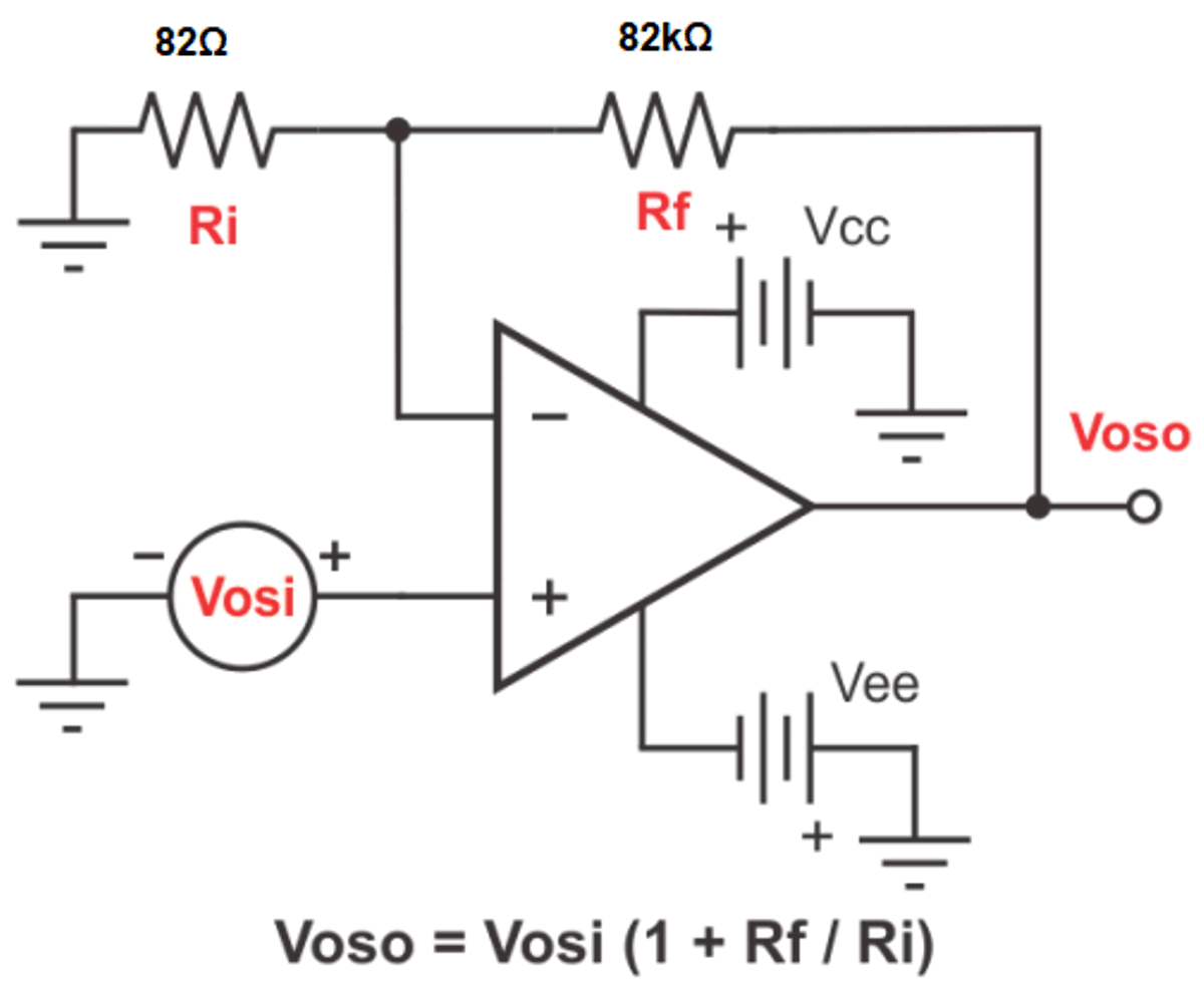
Figure 2-1 shows how the offset voltage can be modeled as a DC voltage generator Vosi, in series with the non-inverting input of an op amp. The exact value of Vosi will vary between components and can have either positive or negative polarity. Typical and maximum Vosi values are specified in the op amp’s datasheet Electrical Characteristics table.
 Figure 2-1 Amplifier stage with voltage offset model
There is always a DC error voltage at the output of an amplifier circuit. This output error is mainly caused by the Vosi multiplied by the non-inverting gain of the amplifier circuit, which appears on the output as Voso. A higher gain circuit will produce a greater Voso at the output.
There are additional factors that add to the total DC output error; finite common-mode rejection (CMRR), power supply rejection (PSRR), open-loop gain (Aol), and input bias currents (Ib) flowing through the source resistances. Although they must be considered in every design, in the interest of brevity, these errors will not be included in this discussion.