SBOA444 November 2020 TMCS1100
3.2 MSP432 LaunchPad Connections
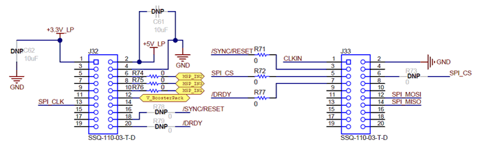
This design has a LaunchPad connector that allows supporting connections to different microcontrollers. The Implemented LaunchPad Connections figure shows the implementation of the LaunchPad connector in this design:
 Figure 3-6 Implemented LaunchPad™
Connections.
For communication to the MSP432 LaunchPad specifically, the SYNC/RESET pin should be brought out to J33 pin 3, SPI_CS should be brought out to J33 pin 5, and DRDY should be brought out to J33 pin 7. These connections to the MSP432 LaunchPad is supported by populating resistors R71, R72, and R77 while depopulating resistors R78, R79, and R73, as is shown in the Implemented LaunchPad Connections figure.
The LaunchPad Connection Mappings table shows the connections that are used on the MSP432 LaunchPad for this design:
| LaunchPad™ PIN | FUNCTION |
|---|---|
| J33 pin 7 (P5.6) | ADS131M08 DRDY |
| J33 pin 5 (P2.4) | ADS131M08 Chip Select |
| J33 pin 3 (P2.6) | ADS131M08 Reset/Sync |
| J33 pin 12 (P1.6) | ADS131M08 DIN (UCB0SIMO) |
| J32 pin 13 (P1.5) | ADS131M08 SPI Clock |
| J33 pin 14 (P1.7) | ADS131M08 DOUT(UCB0SOMI) |
| J33 pin 13 (P2.3) | EUSCIA0 UART RX for PC GUI communication |
| J33 pin 4 (P2.5) | EUSCIA0 UART RX for PC GUI Communication |
| J32 pin 15 (P4.6) | Active Energy Pulse Output |
| J32 pin 10 (P4.2) | Reactive Energy Pulse Output |
| J32 pin 14 (P4.5) | Voltage Zero Crossing Pin |