SBOA553A August 2022 – January 2023 OPA593
3 Bench Test Results
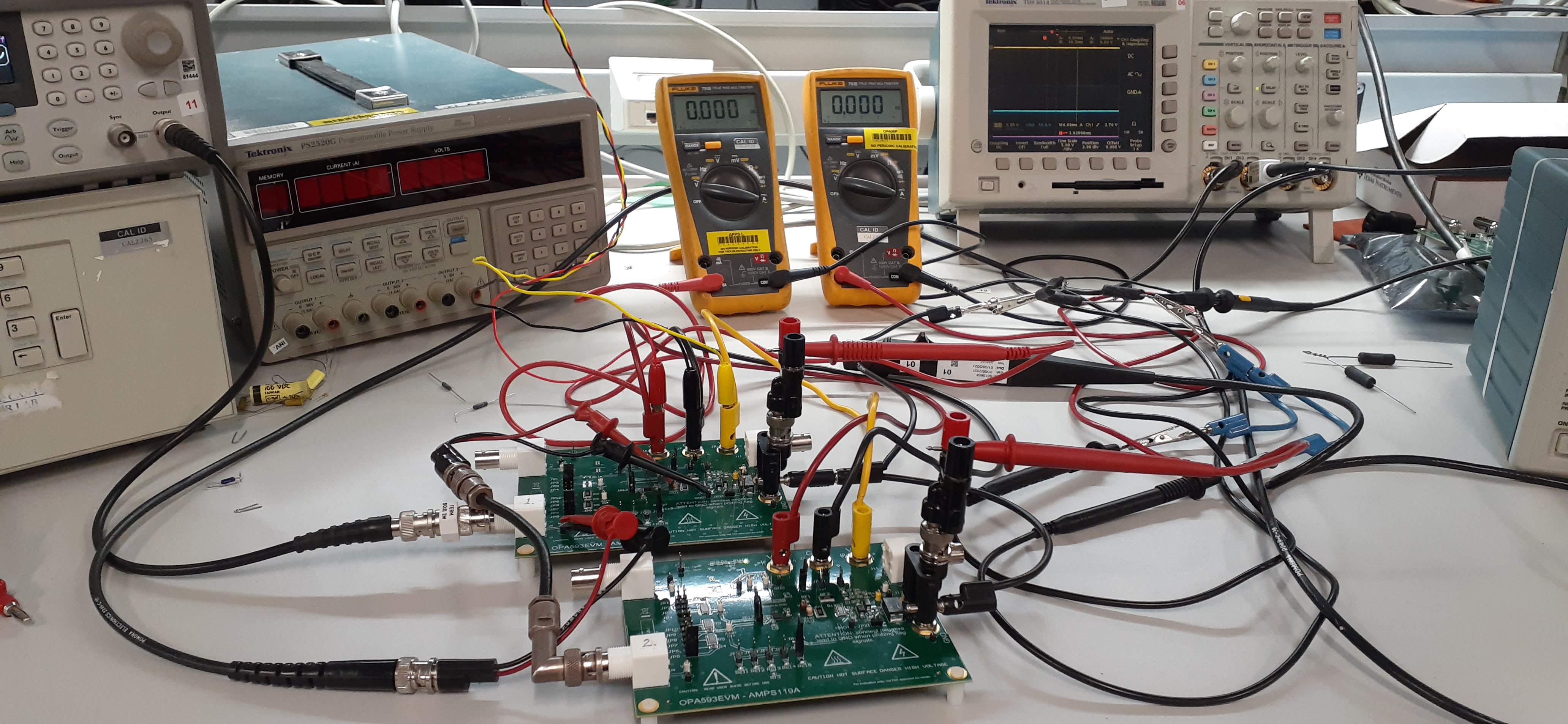
The final test circuit of Figure 2-1 was realized by connecting two OPA593EVM evaluation modules together. The bench tests were intended to evaluate the OPA593 parallel 0.5-A output current capability, and to observe the output behaviors when loaded with different RL and CL loads. Figure 3-1 shows the two EVMs and the bench test equipment setup ready for testing.
 Figure 3-1 OPA593 Parallel Output Test
Setup
Figure 3-1 OPA593 Parallel Output Test
SetupThe first test evaluated a sine-wave output of 0 to 50 V, developed across a 100 Ω, 20 W resistive load. This equated to 0.5-A peak output current. The OPA593EVM power supplies were set to +55 V and –5 V, and current-limit Rset resistors were set to 2.29 kΩ to set the maximum output current limit to about 250 mA for each OPA593EVM. Current limiting should then occur within the OPA593 ±5% rated limit is exceeded. The input stimulus was +2.5 Vdc, plus a 5 Vpp 1-kHz sine wave.
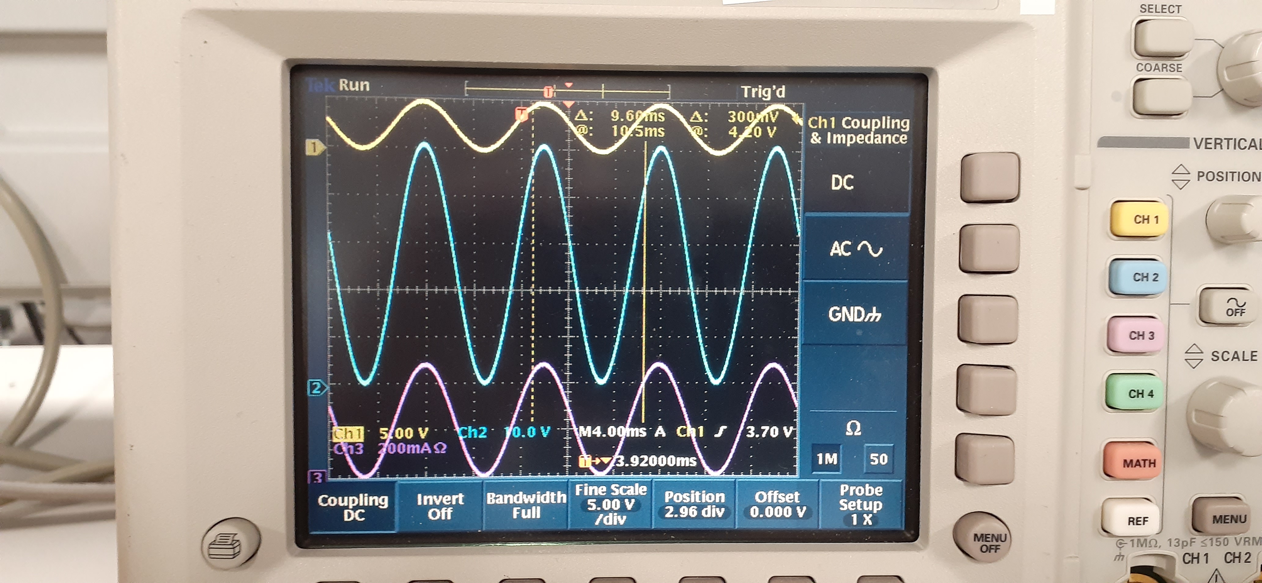
In Figure 3-2 the top trace is the +2.5 Vdc, plus a 5 Vpp 1-kHz sine measured at the U1 non-inverting input. The middle trace is the output sine waveform coming from the two OPA593 parallel outputs producing a peak-to-peak output that extends from 0 V to 50 V. The lower trace is a 200 mA/div current measurement acquired using a Tek TCPA300 AC/DC current probe. The trace verifies that a peak 0.5-A current is being produced by the parallel output amplifier when driving the 100-Ω load.
 Figure 3-2 OPA593 Parallel Output Op Amp
0.5-A Peak Test Result
Figure 3-2 OPA593 Parallel Output Op Amp
0.5-A Peak Test ResultAn attempt to drive the circuit harder and produce more output current resulted in one or both of the OPA593 op amps hitting their user-established automatic current limit of approximately 250 mA. The OPA593 EVM current-limit LED turned on when the internal current limit of the op amp was activated. As a consequence, the output sine wave became clipped on the current peaks verifying the current limiting was activated. This current-limit feature provides protection for both the OPA593 and the load it is driving.
The final test conducted was to observe the OPA593 parallel output behavior when driving a 1-µF, 500-Ω parallel load. The compensation was optimized to drive this particular load as mentioned previously.
An indirect method that can be applied to evaluate the phase margin of an op-amp circuit involves a small-signal transient overshoot test (dominant 2-pole system). This test is presented in TI's Analog Engineer’s Pocket Reference Guide in the Amplifier section. The test applies a low-level step, or square-wave to the input of the amplifier. The output step is kept to about 50- to 100-mV peak to avoid slew rate limiting. Then, the overshoot amplitude is measured relative to the settled output amplitude. Figures 46 and 47 in the pocket reference guide show how the phase margin is estimated from a graph.
A phase margin of 45° provides sufficient margin for many applications and also provides stable operation. A phase margin of 45° correlates with an overshoot of approximately 25% as shown in the graph in Figure 47 of the pocket reference guide. A compensated op amp driving a highly reactive load such as the parallel 500-Ω, 1-µF load, can have even less phase margin because of the very high C-load. Strive to compensate it for a minimum phase margin of no less than 30°. Transient behaviors degrade with low phase margin resulting in high overshoot and long settling times. Their degradation can become an issue that places limits on the dynamic performance of a system.
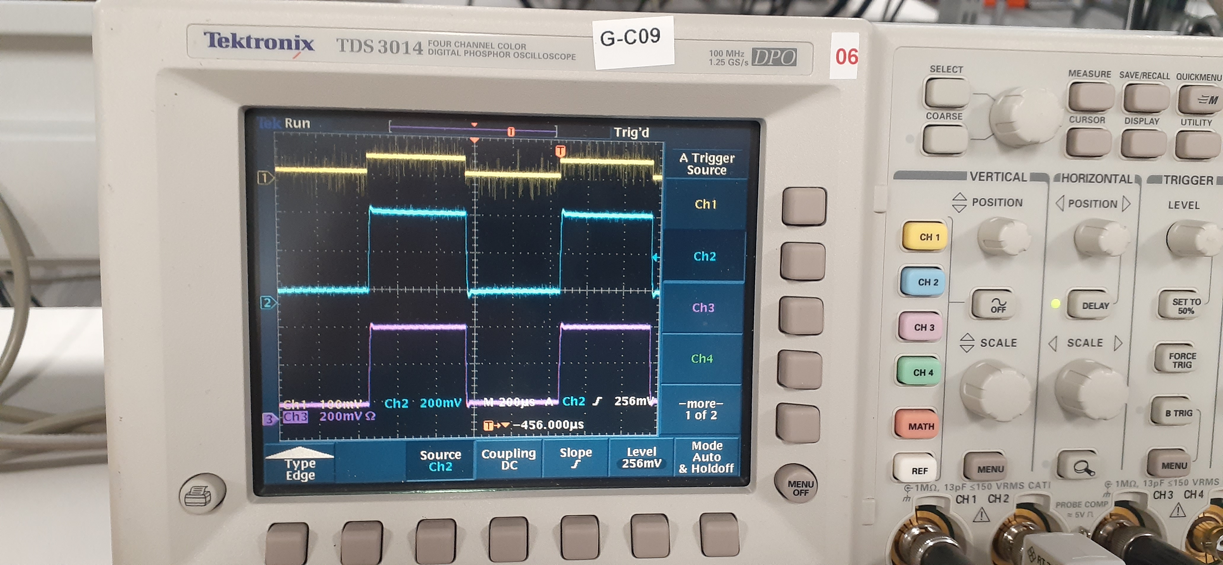
Figure 3-3 shows the small-signal transient response obtained from the OPA593 parallel output amplifier when driving the 1-µF, 500-Ω parallel load. The blue output voltage and pink output current traces exhibit only a small amount of overshoot and fast settling. This result supports a phase margin that is closer to 50° to 60°. That is, the margin is higher than the simulation results that produced approximately 40° for U1, and lower than 70° for U2. The OPA593 model provides a close approximation of the electrical performances of the amplifier and comes close to the correct answer. However, the bench measurement provides a more thorough system evaluation that uses the actual OPA593 op amps.
 Figure 3-3 OPA593 Parallel Output Op Amp
Small Signal Transient Response
Figure 3-3 OPA593 Parallel Output Op Amp
Small Signal Transient ResponseTests conducted with a large signal, square-wave output while driving a high-capacitive load of hundreds of nanofarads and 1 µF caused dim lighting of the OPA593EVM current-limit LEDs. The LED response was determined to be the result of the output current attempting to exceed the 250 mA set current limit of each EVM. This occurred during the transition of the output square wave from low level to high level. It was simply a matter of the edge transition current of the square wave, i = C dv/dt. The faster the edge rate, the higher the instantaneous current is for a particular load capacitance. The LED lighting was the result of the current limiting during the dv/dt event period.