SBOT047 October 2023 INA851
Introducing the first instrumentation amplifier with fully-differential outputs (INAFDA) in the industry, the INA851. The INA851 integrates a two-amplifier input gain stage and a differential amplifier output stage into a one-chip solution. The INA851 redefines the instrumentation amplifier landscape by offering an integrated design within the performance and price range of a discrete design.
 Figure 1 INA851 ADC Driver
Application
Figure 1 INA851 ADC Driver
ApplicationDesign Considerations
- Input overvoltage protection of up to ±40 V
- Attenuating gain down to 0.2 V and up to a gain of 10,000
- Single external resistor to set gain
- External access pin for additional noise filtering
The output driver has a built-in clamping circuit, featuring an integrated low-dropout (LDO), designed to protect the succeeding signal chain, typically an analog-to-digital converter (ADC). When connecting the ADC power supply pins to the INA851 clamp pins, the INA851 output voltage is clamped at 600 mV above the ADC power supply voltage to protect the ADC and downstream devices against overdrive damage, without experiencing distortion.
 Figure 2 Simplified Schematic of Output
Driver Clamping Structure
Figure 2 Simplified Schematic of Output
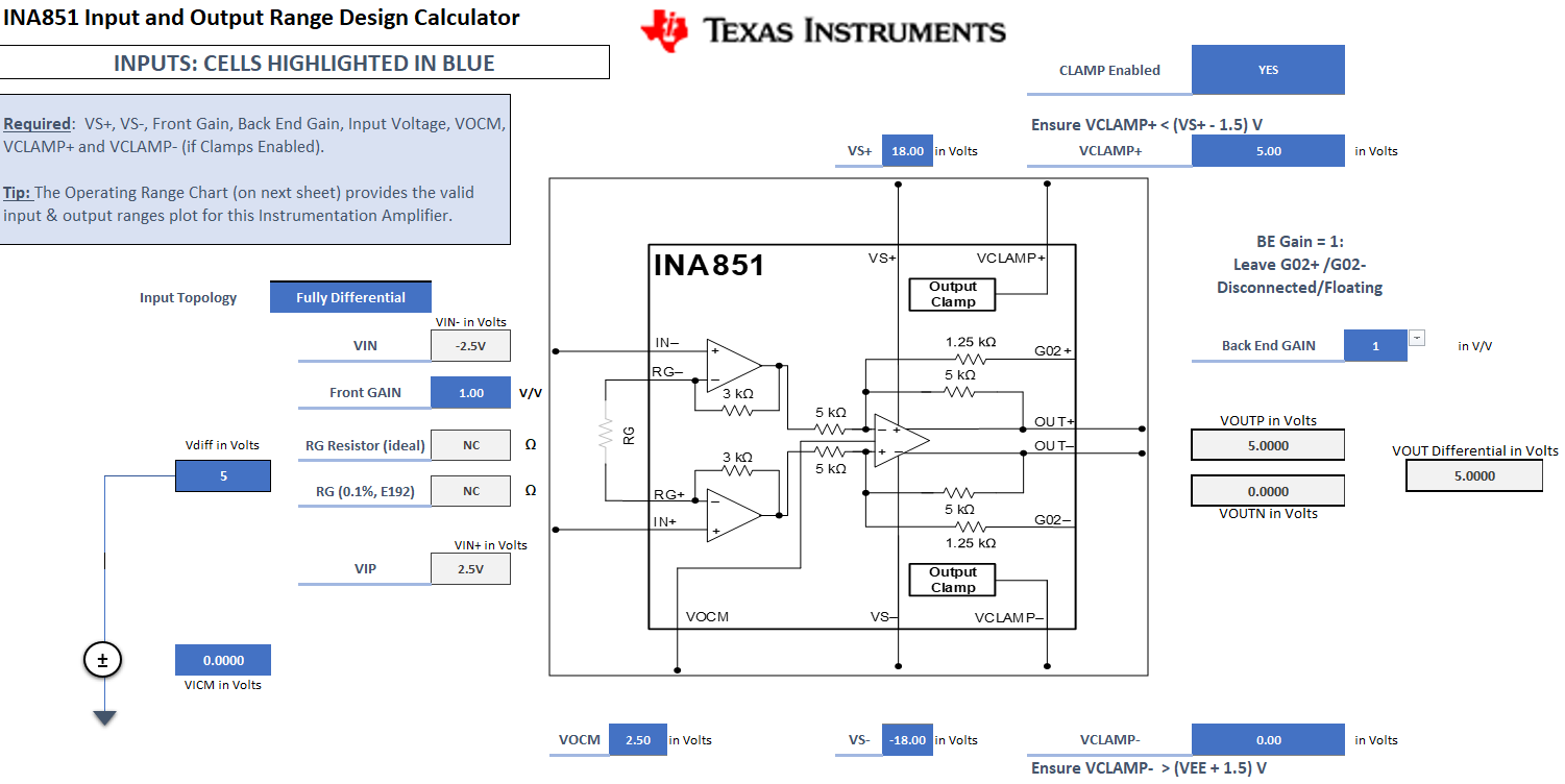
Driver Clamping StructureDue to the additional LDO functionality in the output stage, the input and output range calculation comes with more complexity compared to traditional INAs. To help understand the device functionality and ease device implementation, TI created the INA851 Input and Output Range Design Calculator, available for download online. The tool calculates the input and output range based on the power supply voltage, as well as input common mode range and differential output based on user inputs. The calculator also provides a visual graphical display of the resulting range, to better highlight device versatility. Figure 3 shows the GUI in the calculator.
 Figure 3 INA851 Input and Output Range
Design Calculator
Figure 3 INA851 Input and Output Range
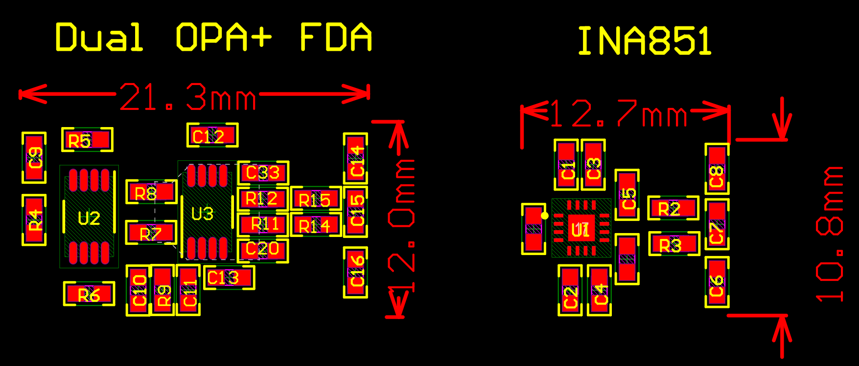
Design CalculatorThe integrated design offered by the INA851 also incorporates precision ratiometric resistors in the FDA output stage, improving accuracy while reducing the errors due to resistor mismatch. Overall, the INA851 reduces design component count, in turn reducing printed-circuit-board (PCB) area compared to discrete solutions by 46%, based on a typical strain gauge application. Figure 4 compares a typical discrete design layout including the dual op-amp input gain stage, differential driving amplifier, resistor network, and decoupling capacitors, resulting in a total design size of 255.6 mm² compared to the INA851 integrated design size of 137.16 mm².
 Figure 4 PCB Size Comparison
| Part Number(1) | Maximum Operating Voltage | Features |
|---|---|---|
| INA851 | 36 V | Low-noise (3.2 nV/√Hz) high-speed (22 MHz) fully-differential instrumentation amplifier with OVP (±40 V) |
| INA849 | 36 V | Single-ended, ultra-low noise (1 nV/√Hz), high-speed (28 MHz, 35 V/μs), precision (35 μV) instrumentation amplifier |
| PGA855 | 36 V | Low-noise, wide-bandwidth, fully-differential-output programmable-gain instrumentation amplifier |
For additional assistance, ask questions to TI engineers on the TI E2E™ Amplifier Support Forum.