SBOU162A March 2017 – May 2017
-
DIYAMP-SOIC-EVM
- Trademarks
- 1 Introduction
- 2 Hardware Setup
- 3
Schematic and PCB Layout
- 3.1 Schematic PCB Drawing
- 3.2 Single-Supply, Multiple Feedback Filter
- 3.3 Single-Supply, Sallen-Key Filter
- 3.4 Single-Supply, Non-Inverting Amplifier
- 3.5 Single-Supply, Inverting Amplifier
- 3.6 Difference Amplifier
- 3.7 Dual-Supply, Multiple Feedback Filter
- 3.8 Dual-Supply, Sallen-Key Filter
- 3.9 Inverting Comparator
- 3.10 Non-Inverting Comparator
- 3.11 Riso With Dual Feedback
- 3.12 Dual-Supply, Non-Inverting Amplifier
- 3.13 Dual-Supply, Inverting Amplifier
- 4 Connections
- 5 Bill of Materials and Reference
- Revision History
3.5 Single-Supply, Inverting Amplifier
Figure 18 shows the schematic for the single-supply, inverting amplifier circuit configuration.
 Figure 18. Single-Supply, Inverting Amplifier Schematic
 The inverting op-amp configuration takes an input signal that is applied directly to the inverting input terminal and outputs a signal that is the opposite polarity as the input signal. The benefit of this topology is that it avoids common mode limitations. The load resistance for this topology is equal to R2. The values of the resistors in the feedback network will determine the amount of gain to amplify the input signal.
The single-supply, inverting amplifier circuit provides the option to AC couple the input, filter the output, and bias the output of the amplifier to a desired value.
Equation 9 displays the dc transfer function of the single-supply, inverting amplifier circuit configuration.
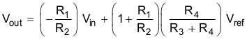
- C3 is shorted with a 0-Ω resistor
where
Capacitor C3 provides the option to AC couple the input of the single-supply, inverting amplifier by creating a high-pass filter. Equation 10 displays the dc transfer function of the single-supply, inverting amplifier circuit configuration.
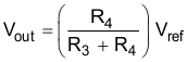
- The input is AC coupled with C3
where
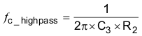
The cutoff frequency of the high-pass filter can be calculated using Equation 11.
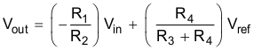
Equation 12 displays the transfer function when the frequency of the input signal is above the cutoff frequency calculated in Equation 11.
Capacitor C2 filters noise that may be introduced from the Vref input. Equation 13 calculates the cutoff frequency due to C2.
Capacitor C4 provides the option to filter the output. The cutoff frequency of the filter can be calculated using Equation 14.
The PCB layout of the top layer of the single-supply, inverting amplifier circuit configuration is displayed in Figure 19.
 Figure 19. Single-Supply, Inverting Amplifier Top Layer
 The PCB layout of the bottom layer of the single-supply, inverting amplifier circuit configuration is displayed in Figure 20.
 Figure 20. Single-Supply, Inverting Amplifier Bottom Layer