SBOU162A March 2017 – May 2017
-
DIYAMP-SOIC-EVM
- Trademarks
- 1 Introduction
- 2 Hardware Setup
- 3
Schematic and PCB Layout
- 3.1 Schematic PCB Drawing
- 3.2 Single-Supply, Multiple Feedback Filter
- 3.3 Single-Supply, Sallen-Key Filter
- 3.4 Single-Supply, Non-Inverting Amplifier
- 3.5 Single-Supply, Inverting Amplifier
- 3.6 Difference Amplifier
- 3.7 Dual-Supply, Multiple Feedback Filter
- 3.8 Dual-Supply, Sallen-Key Filter
- 3.9 Inverting Comparator
- 3.10 Non-Inverting Comparator
- 3.11 Riso With Dual Feedback
- 3.12 Dual-Supply, Non-Inverting Amplifier
- 3.13 Dual-Supply, Inverting Amplifier
- 4 Connections
- 5 Bill of Materials and Reference
- Revision History
3.4 Single-Supply, Non-Inverting Amplifier
Figure 15 shows the schematic for the single-supply, non-inverting amplifier circuit configuration.
 Figure 15. Single-Supply, Non-Inverting Amplifier Schematic
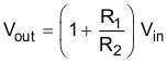
 The non-inverting op-amp configuration takes an input signal that is applied directly to the high impedance, non-inverting input terminal and outputs a signal that is the same polarity as the input signal. The load resistance for this topology is the sum of R1 and R2. The values of the resistors in the feedback network will determine the amount of gain to amplify the input signal.
There are multiple ways to configure the single-supply, non-inverting amplifier. The following cases show three primary use case configurations for this circuit.
Case 1: Standard non-inverting circuit
This circuit board can be configured into a standard non-inverting circuit by shorting C3 and C4 with a 0-Ω resistor and leaving R3 and R4 unpopulated.
Equation 2 displays the transfer function for the standard single-supply, non-inverting amplifier circuit configuration.
- C3 is shorted with a 0-Ω resistor
- C4 is shorted with a 0-Ω resistor
- R3 is unpopulated
- R4 is unpopulated
where
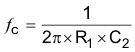
Capacitor C2 provides the option to filter the output. The cutoff frequency of the filter can be calculated using Equation 3.
Case 2: AC coupled, single-supply, non-inverting circuit
This circuit board can be configured into an AC coupled non-inverting circuit by populating C3 and C4 with capacitors and populating R3 or R4 with resistors. R3 and R4 are used to set the DC output in the following two ways:
Option 1: VREF is directly applied to the input IN+
- R3 is populated with the desired biasing resistor
- R4 is unpopulated
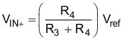
Option 2: VREF is divided down and applied to the input IN+
- R3 and R4 are populated with resistors, see Equation 4
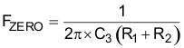
The AC response of the input signal is high-passed through C4, R3 + R4. The op-amp noise-gain is unity-gain until the gain begins to rise at the zero frequency defined in Equation 5.
The gain flattens off to the same gain defined in Equation 2 at the frequency defined in Equation 6.
For more information on the AC coupled non-inverting circuit, see e2e.ti.com.
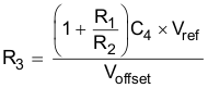
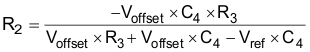
Case 3: Non-inverting signal scaling circuit
This circuit board can be configured into a non-inverting signal scaling circuit by shorting C3 with a 0-Ω resistor and populating C4 with a resistor. This forms a 3-resistor divider with R3 and R4 on the input to scale or shift the input signal level. The op amp is typically configured as a unity-gain buffer.
- Choose a value for the resistor installed in place of C4
- Compute R3
- Compute R2
For more information on the AC coupled non-inverting circuit, see e2e.ti.com.
The PCB layout of the top layer of the single-supply, non-inverting circuit configuration is displayed in Figure 16.
 Figure 16. Single-Supply, Non-Inverting Amplifier Top Layer
 The PCB layout of the bottom layer of the single-supply, non-inverting circuit configuration is displayed in Figure 17.
 Figure 17. Single-Supply, Non-Inverting Amplifier Bottom Layer