SBVA092 June 2022 TPS7A14
3.1 Simulated Bode Plot vs. Evaluated Bode Plot
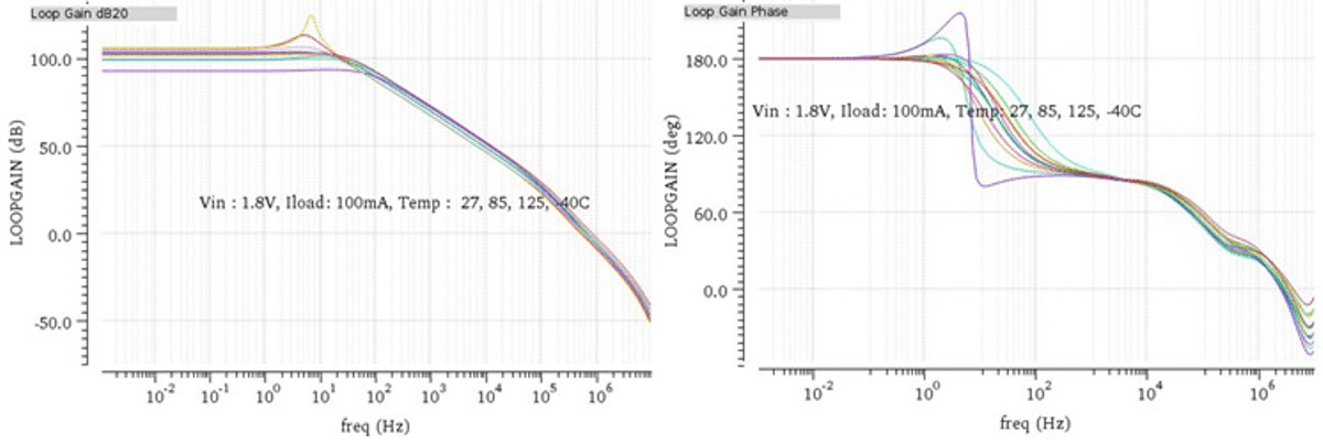
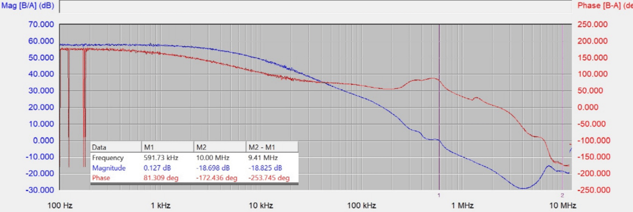
As mentioned in Section 2.2, verifying stability of control loop should include whole operating conditions such as corner cases of silicon variations, temperature range as well. In detail, it also requires considering quiescent current of feedback network and feedforward value. Figure 3-1 is a simulated Gain and Phase plot in product design level. Each curve represents temperature and three CMOS process variation as weak, normal and strong. Simply, it turns out about 540-kHz UGB (unit gain bandwidth) and 35° PM (phase margin) at 100 mA output load current. Meanwhile, same measurement using frequency analyzer on TPS7A1408EVM after modifying schematic with 10nF feedforward capacitor shows UGB of about 590 kHz and 81° PM. It can be left for further tune by users.
 Figure 3-1 Simulated Bode Plot (Vin=1.8 V, Vo=1.2 V, Iout=100 mA)
 Figure 3-2 Evaluated Bode Plot on EVM (Vin=1.8 V, Vo=1.2 V, Iout=100 mA)