SFFS799 March 2024 TLV2365-Q1 , TLV365-Q1
4.1 SOT-23 Package
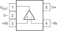
Figure 4-1 shows the TLVx365-Q1 pin diagram for the SOT-23 package. For a detailed description of the device pins, see the Pin Configuration and Functions section in the TLVx365-Q1 data sheet.
 Figure 4-1 Pin Diagram (SOT-23) Package
Table 4-2 Pin FMA for Device Pins
Short-Circuited to Ground
| Pin Name | Pin No. | Description of Potential Failure Effect(s) | Failure Effect Class |
|---|---|---|---|
| VOUT | 1 | Short to GND may cause device to overheat. | B |
| V- | 2 | Normal operation, unless dual supply voltage was intended. | D |
| +IN | 3 | Input at V- (GND) is valid input, however, desired application result is unlikely. | C |
| -IN | 4 | Input at V- (GND) is valid input, however, desired application result is unlikely. | C |
| V+ | 5 | Diodes from input to V+ may turn on due to input signal and cause electrical overstress (EOS). | A |
Table 4-3 Pin FMA for Device Pins
Open-Circuited
| Pin Name | Pin No. | Description of Potential Failure Effect(s) | Failure Effect Class |
|---|---|---|---|
| VOUT | 1 | Output can be left open. There is no effect on the device, but the output will not be measured. | C |
| V- | 2 | Lowest voltage output pin will try to power the V- pin of the device. | B |
| +IN | 3 | Floating input, circuit will likely not function as expected. | C |
| -IN | 4 | Floating input, circuit will likely not function as expected. | C |
| V+ | 5 | Highest voltage output pin will try to power the V+ pin of the device. | B |
Table 4-4 Pin FMA for Device Pins
Short-Circuited to Adjacent Pin
| Pin Name | Pin No. | Shorted to | Description of Potential Failure Effect(s) | Failure Effect Class |
|---|---|---|---|---|
| VOUT | 1 | V- | Short to V- may cause device to overheat. | B |
| V- | 2 | +IN | Input at V- (GND) is valid input, however, desired application result is unlikely. | C |
| +IN | 3 | -IN | No damage to device. Application circuit will not work. Pins are not adjacent to each other. | C |
| -IN | 4 | V+ | Input at V+ is a valid input, however, desired application result is unlikely. Pins are not as near to each other, due to package type. | B |
| V+ | 5 | VOUT | Short to VS+ may cause device to overheat. Pins are not adjacent to each other. | B |
Table 4-5 Pin FMA for Device Pins
Short-Circuited to V+
| Pin Name | Pin No. | Description of Potential Failure Effect(s) | Failure Effect Class |
|---|---|---|---|
| VOUT | 1 | Short to V+ may cause device to overheat. | B |
| V- | 2 | Diodes from input to V- may turn on due to input signal and cause electrical overstress (EOS). | A |
| +IN | 3 | Input at V+ is a valid input, however, desired application result is unlikely. | C |
| -IN | 4 | Input at V+ is a valid input, however, desired application result is unlikely. | C |
| V+ | 5 | Normal Operation. | D |