SFFS821 March 2024 SN74AXC4T774-Q1
4 Pin Failure Mode Analysis (Pin FMA)
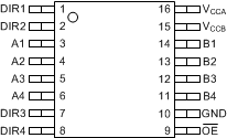
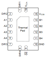
This section provides a failure mode analysis (FMA) for the pins of the SN74AXC4T774-Q1 (TSSOP and VQFN packages). The failure modes covered in this document include the typical pin-by-pin failure scenarios:
- Pin short-circuited to ground (see Table 4-2 )
- Pin open-circuited (see Table 4-3)
- Pin short-circuited to an adjacent pin (see Table 4-4)
- Pin short-circuited to supply (see Table 4-5 and Pin FMA for Devices Short-Circuited to VCCB)
Table 4-2 through Pin FMA for Devices Short-Circuited to VCCB also indicate how these pin conditions can affect the device as per the failure effects classification in Table 4-1.
Table 4-1 TI Classification of Failure Effects
| Class | Failure Effects |
|---|---|
| A | Potential device damage that affects functionality |
| B | No device damage, but loss of functionality |
| C | No device damage, but performance degradation |
| D | No device damage, no impact to functionality or performance |
Figure 4-1, Figure 4-2, and Figure 4-3 show the SN74AXC4T774-Q1 pin diagrams for the TSSOP, VQFN, and UQFN packages. For a detailed description of the device pins, see the Pin Configuration and Functions section in the SN74AXC4T774-Q1 data sheet.
 Figure 4-1 Pin Diagram (TSSOP) Package
 Figure 4-2 Pin Diagram (VQFN Package)
 Figure 4-3 Pin Diagram (UQFN Package)
Table 4-2 Pin
FMA for Device Pins Short-Circuited to
Ground
| Pin Name | Pin No. | Description of Potential Failure Effects | Failure Effect Class |
|---|---|---|---|
| DIR1 | 1 | Direction control will fix B --> A direction | B |
| DIR2 | 2 | ||
| A1 | 3 | If configured as an output then damage is possible. If configured as input, no damage, but output will not switch | A |
| A2 | 4 | ||
| A3 | 5 | ||
| A4 | 6 | ||
| DIR3 | 7 | Direction control will fix B --> A direction | B |
| DIR4 | 8 | ||
| ŌĒ | 9 | All outputs will be active, device cannot be disabled | B |
| GND | 10 | Normal Operation | D |
| B4 | 11 | If configured as an output then damage is possible. If configured as input, no damage, but output will not switch | A |
| B3 | 12 | ||
| B2 | 13 | ||
| B1 | 14 | ||
| VCCB | 15 | GND short to VCC, device will be bypassed - may cause system damage, but not device damage | B |
| VCCA | 16 |
Table 4-3 Pin
FMA for Device Pins Open-Circuited
| Pin Name | Pin No. | Description of Potential Failure Effect(s) | Failure Effect Class |
|---|---|---|---|
| VCCA | 16 | GND short to VCC, device will be bypassed; can cause system damage, but not device damage | B |
| GND | 10 | Device will not be powered | B |
| A | 3-6 | If configured as an output then damage is possible. If configured as input, no damage, but output will not switch | B |
| B | 11-14 | If configured as an output then damage is possible. If configured as input, no damage, but output will not switch | B |
| DIR | 1-2 7-8 | Direction control will fix B --> A direction | B |
| VCCB | 15 | GND short to VCC, device will be bypassed; can cause system damage, but not device damage | B |
Table 4-4 Pin FMA for Device Pins
Short-Circuited to Adjacent Pin
| Pin Name | Pin No. | Shorted to | Description of Potential Failure Effects | Failure Effect Class |
|---|---|---|---|---|
| DIR1 | 1 | DIR2 | If both HIGH, direction control will fix A --> B direction. If both LOW, direction control will fix B --> A direction. If one DIR is HIGH and the other is LOW, bus contention during transitions could occur and may cause high current | A |
| DIR2 | 2 | A1 | If DIR2 is LOW, A2 will be an output and damage is possible. If DIR3 is HIGH, A2 will be an input and drive the output B2 LOW | A |
| A1 | 3 | A2 | If A(n) and A(n+1) are configured as outputs then damage is possible. If configured as inputs, both bits will always have the same value | A |
| A2 | 4 | A3 | ||
| A3 | 5 | A4 | ||
| A4 | 6 | DIR3 | If DIR3 is LOW, A3 will be an output and damage is possible. If DIR3 is HIGH, A3 will be an input and drive the output B3 LOW | A |
| DIR3 | 7 | DIR4 | If both HIGH, direction control will fix A --> B direction. If both LOW, direction control will fix B --> A direction. If one DIR is HIGH and the other is LOW, bus contention during transitions could occur and may cause high current | A |
| DIR4 | 8 | ŌĒ | If ŌĒ is HIGH, I/Os will be placed in Hi-Z. If both DIR and ŌĒ are LOW, direction control will fix B --> A direction. If DIR is HIGH and the ŌĒ is LOW, direction control will fix A --> B direction. | B |
| ŌĒ | 9 | GND | All outputs will be active; device cannot be disabled | B |
| GND | 10 | B4 | If B4 is configured as an output then damage is possible. If configured as input, output A4 will be fixed LOW | A |
| B4 | 11 | B3 | If B(n) and B(n+1) are configured as outputs then damage is possible. If configured as inputs, both bits will always have the same value. | A |
| B3 | 12 | B2 | ||
| B2 | 13 | B1 | ||
| B1 | 14 | VCCB | If B1 is configured as an output then damage is possible. If configured as input, no damage, but output A1 will remain high. | A |
| VCCB | 15 | VCCA | GND short to VCC, device will be bypassed; may cause system damage, but not device damage | B |
| VCCA | 16 | DIR1 | Direction control will fix A --> B direction | B |
Table 4-5 Pin
FMA for Device Pins Short-Circuited to
VCCA
| Pin Name | Pin No. | Description of Potential Failure Effect(s) | Failure Effect Class |
|---|---|---|---|
| VCCA | 16 | Normal Operation | D |
| GND | 10 | GND short to VCC, device will be bypassed; may cause system damage, but not device damage | B |
| A | 3-6 | If configured as an output then damage is possible. If configured as input, no damage, but output will not switch | A |
| B | 11-14 | If configured as an output then damage is possible. If configured as input, damage is possible if VIH/VIL not met | A |
| DIR | 1-2, 7-8 | Direction control will fix A --> B direction | B |
| ŌĒ | 9 | I/Os will be placed in Hi-Z | B |
| VCCB | 15 | VCCA short to VCCB, device will be bypassed; may cause system damage, but not device damage | B |
Table 4-6 Pin FMA for Device Pins
Short-Circuited to VCCB
| Pin Name | Pin No. | Description of Potential Failure Effect(s) | Failure Effect Class |
|---|---|---|---|
| VCCA | 16 | VCCA short to VCCB, device will be bypassed; can cause system damage, but not device damage | B |
| GND | 10 | GND short to VCC, device will be bypassed; can cause system damage, but not device damage | B |
| A | 3-6 | If configured as an output then damage is possible. If configured as input, damage is possible if VIH/VIL not met | A |
| B |
11-14 |
If configured as an output then damage is possible. If configured as input, no damage, but output will not switch | A |
| DIR | 1-2, 7-8 | If VCCB>VCCA, DIR will fix B --> A direction OR if VCCB < VCCA, input could be inappropriate logic level potentially causing damage | B |
| ŌĒ | 9 | I/Os will be placed in Hi-Z | B |
| VCCB | 15 | Normal Operation | D |