SLAA916A November 2019 – March 2020 MSP430FR2310 , MSP430FR2311 , MSP430FR2353 , MSP430FR2355
Design Goals
| AC Gain | Filter Cut-Off Frequency | Supply | ||
|---|---|---|---|---|
| 90 dB | fL | fH | Vcc | Vee |
| 0.7 Hz | 10 Hz | 3.3 V | 0 V | |
Design Description
Some MSP430™ microcontrollers (MCUs) contain configurable integrated signal chain elements such as op-amps, DACs, and programmable gain stages. These elements make up a peripheral called the Smart Analog Combo (SAC). For information on the different types of SACs and how to leverage their configurable analog signal chain capabilities, visit MSP430 MCUs Smart Analog Combo Training. To get started with your design, download the Low-Noise Long-Range PIR Sensor Conditioner Circuit Design Files.
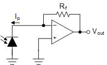
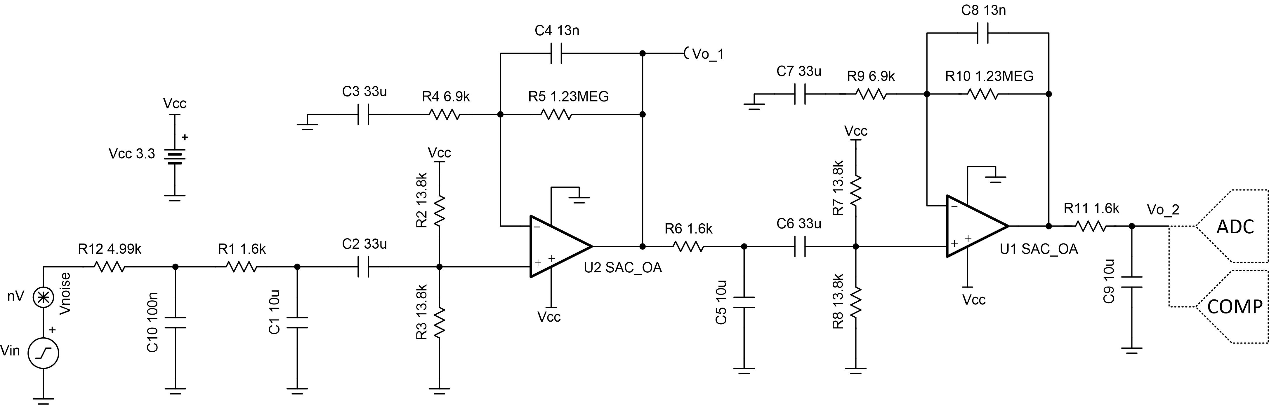
This design leverages two of the four integrated op-amp blocks (SACs) in the MSP430FR2355 MCU. Two SAC_L3 peripherals are configured as cascaded op-amps in general-purpose mode to amplify and filter the signal from a passive infrared (PIR) sensor. The circuit includes multiple low-pass and high-pass filters to reduce noise at the output of the circuit to be able to detect motion at long distances and reduce false triggers. The output of the second-stage op-amp in this circuit can be internally or externally connected to other integrated peripherals in the MSP430FR2355 MCU. For example, the analog-to-digital converter (ADC) window comparator can sample this output periodically (with no CPU intervention) and trigger an interrupt when the signal crosses a threshold, indicating motion or an alert.
Design Notes
- The common-mode voltage and output-bias voltage are set using the resistor dividers between R2 and R3 (and R7 and R8).
- Two or more amplifier stages must be used to allow for sufficient loop gain.
- Additional low-pass and high-pass filters can be added to further reduce noise.
- Capacitors C4 and C8 filter noise by decreasing the bandwidth of the circuit and help stabilize the amplifiers.
- RC filters on the output of the amplifiers (for example, R6 and C5) are required to reduce the total integrated noise of the amplifier.
- The maximum gain of the circuit can be affected by the cut-off frequencies of the filters. The cut-off frequencies may need to be adjusted to achieve the desired gain.
- For this design, two SAC_L3 peripherals in the MSP430FR2355 MCU are configured as cascaded op-amps in general-purpose mode.
- This design can also be implemented by using the transimpedance amplifier (TIA) and SAC_L1 peripheral in the MSP430FR2311 MCU for the cascaded op-amps, but since the maximum input voltage of the TIA is limited to VCC/2, the common-mode voltage and gain should be limited accordingly.
- The Low-Noise Long-Range PIR Sensor Conditioner Circuit Design Files include a code example demonstrating how to properly configure the SAC_L3 and ADC window comparator peripherals in the MSP430FR2355 MCU.
Design Steps
- Choose large-valued capacitors C1, C5, and C9 for the low-pass filters. These capacitors should be selected first because large-valued capacitors have limited standard values to select from compared to standard resistor values.
- Calculate resistor values for R1, R6, and R11 to form the low-pass filters.
- Select capacitor values for C2, C3, C6, and C7 for the high-pass filters.
- Calculate the resistor values for R4 and R9 for the high-pass filters.
- Set the common-mode voltage of the amplifier to mid-supply using a voltage divider. The equivalent resistance of the voltage divider should be equal to R4 to properly set the corner frequency of the high-pass filter.
- Calculate the gain required by each gain stage to achieve the total gain requirement. Distribute the total gain target of the circuit evenly between both gain stages.
- Calculate R5 to set the gain of the first stage.
- Calculate C4 to set the low-pass filter cut-off frequency.
- Since the gain and cut-off frequency of the first gain stage is equal to the second gain stage, set all component values of both stages equal to each other.
- Calculate R11 to set the cut-off frequency of the low-pass filter at the output of the circuit.
Design Simulations
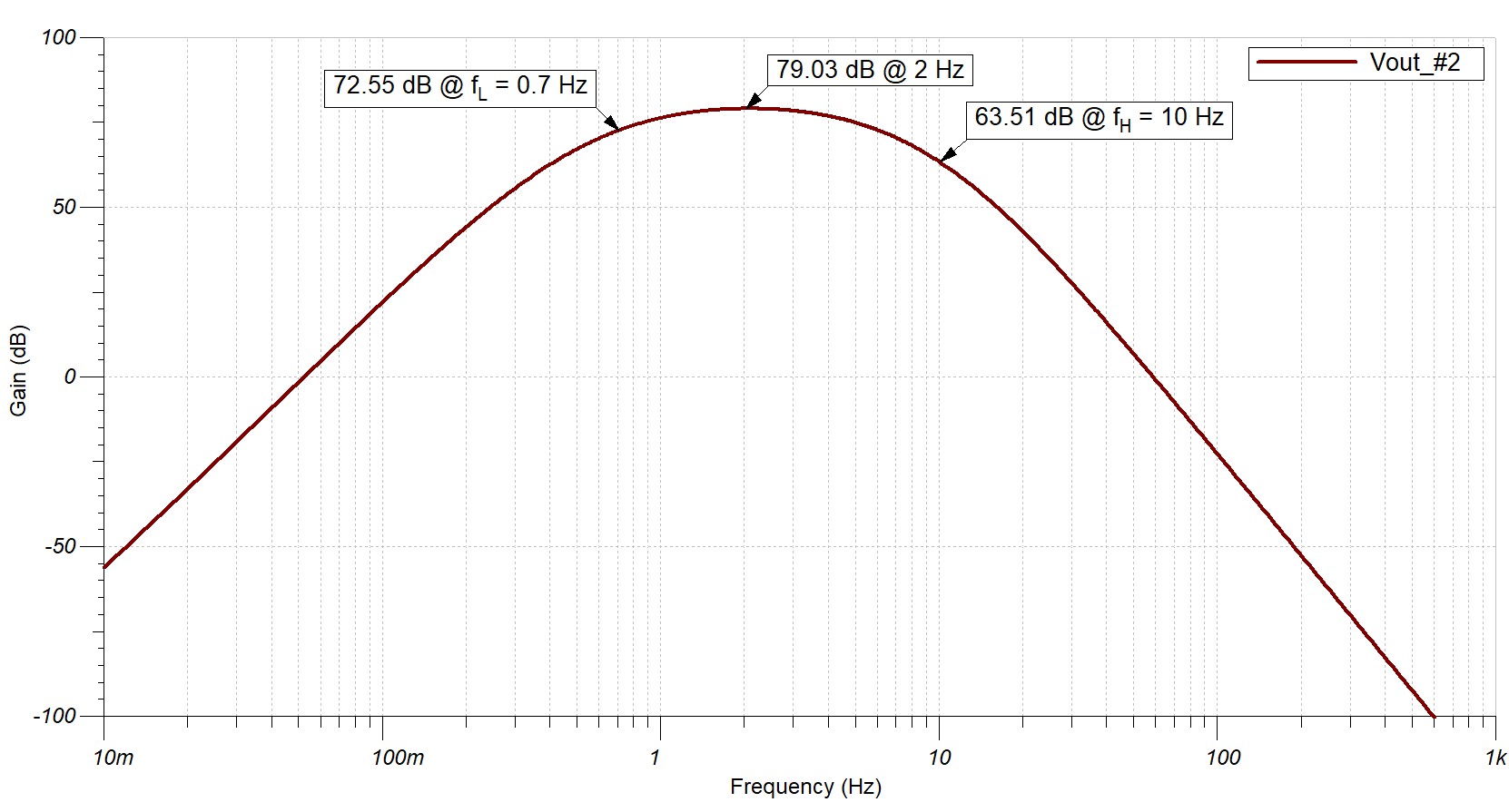
AC Simulation Results
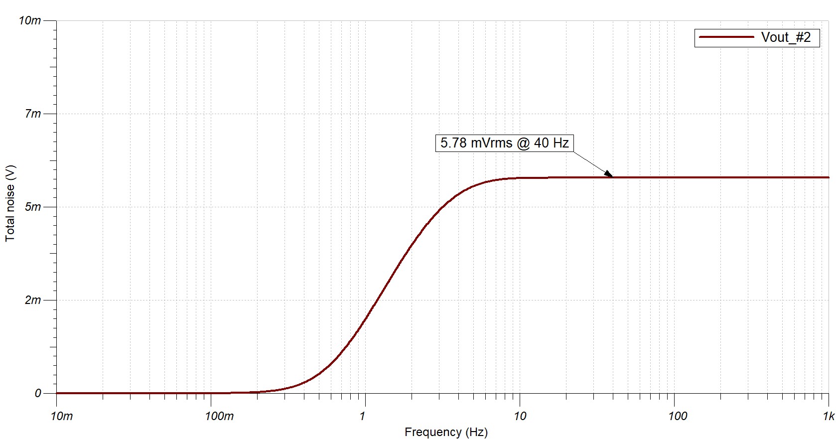
Noise Simulation Results
Target Applications
- Motion detector
- Occupancy detection
- Analog security camera
- IP network camera
- Lighting sensor
- Thermostat
- Video doorbell
References
- Low-Noise Long-Range PIR Sensor Conditioner Circuit Design Files
- Analog Engineer's Circuit Cookbooks
- MSP430FR2311 TINA-TI Spice Model
- How to Use the Smart Analog Combo in MSP430TM MCUs
- MSP430 MCUs Smart Analog Combo Training
| MSP430FRxx Smart Analog Combo | ||
|---|---|---|
| MSP430FR2311 SAC_L1 | MSP430FR2355 SAC_L3 | |
| Vcc | 2.0 V to 3.6 V | |
| VCM | -0.1 V to VCC + 0.1 V | |
| Vout | Rail-to-rail | |
| Vos | ±5 mV | |
| AOL | 100 dB | |
| Iq | 350 µA (high-speed mode) | |
| 120 µA (low-power mode) | ||
| Ib | 50 pA | |
| UGBW | 4 MHz (high-speed mode) | 2.8 MHz (high-speed mode) |
| 1.4 MHz (low-power mode) | 1 MHz (low-power mode) | |
| SR | 3 V/µs (high-speed mode) | |
| 1 V/µs (low-power mode) | ||
| Number of channels | 1 | 4 |
| http://www.ti.com/product/MSP430FR2311 | ||
| http://www.ti.com/product/MSP430FR2355 | ||
Design Alternate Op Amp
| MSP430FR2311 Transimpedance Amplifier | |
|---|---|
| Vcc | 2.0 V to 3.6 V |
| VCM | -0.1 V to VCC/2 V |
| Vout | Rail-to-rail |
| Vos | ±5 mV |
| AOL | 100 dB |
| Iq | 350 µA (high-speed mode) |
| 120 µA (low-power mode) | |
| Ib | 5 pA (TSSOP-16 with OA-dedicated pin input) |
| 50 pA (TSSOP-20 and VQFN-16) | |
| UGBW | 5 MHz (high-speed mode) |
| 1.8 MHz (low-power mode) | |
| SR | 4 V/µs (high-speed mode) |
| 1 V/µs (low-power mode) | |
| Number of channels | 1 |
| http://www.ti.com/product/MSP430FR2311 | |
Related MSP430 Circuits