SLAA946 April 2021 AFE10004
7 Controlled Sequencing With the AFE10004
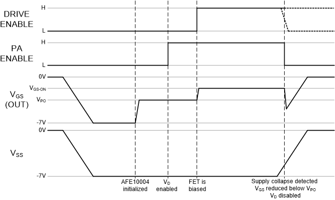
The power sequencing requirements of the PA are maintained by the AFE10004 at start-up. Consider Figure 7-1: as the AFE10004 supplies ramp to normal operating value, the VGS bias (OUT) is connected to the CLAMP output, which tracks the negative supply, VSS. After the supplies are established, the CLAMP and DAC output load the initial values from the LUT. The OUT pin is still connected to the CLAMP value, which has now assumed the pinch-off voltage (step 1 in Figure 3-1). Once the device has loaded the LUT for the outputs from memory, the AFE10004 releases the PA enable signal, which is used to enable the VD supply (step 2). Next, the externally generated drive enable (DRVEN) input switches the OUT pin from the CLAMP output to the DAC output, which is now the temperature compensated VGS voltage (step 3). The RF signal can now be applied to the FET (step 4).
 Figure 7-1 AFE10004 Power Sequence Control
The AFE10004 controls the sequence during power down. When the device receives an alarm input or detects a supply collapse, it connects the OUT pin to the CLAMP output, which brings the VGS to the pinch-off voltage (power down step 2; note that step 1 is controlled by the RF source). Next, the PA enable signal becomes low, which disables the VD supply. Finally, the OUT value tracks the VSS supply until it collapses to ground.