SLAAE20 May 2021 DAC43701 , DAC43701-Q1 , DAC53701 , DAC53701-Q1
Design Description
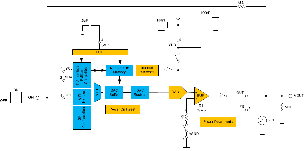
This design uses a buffered voltage output DAC to create a comparator with a programmable threshold value. Additional features such as hysteresis or a latching output can be configured as well. In this design, the integrated buffer will act as a comparator and the output of the DAC will act as the threshold for the comparator. The 8-bit DAC43701, and 10-bit DAC53701 have a general-purpose input pin, GPI, that can be used to trigger a function generator, switch between a high and low DAC value, or power down the DAC. The DAC43701 and DAC53701 integrated buffer has an exposed feedback path via the feedback pin (FB) which will act as the voltage input to the comparator. All register settings can be saved using the non-volatile memory (NVM) on the DAC43701 and DAC53701 meaning that the devices can be used without a processor, even after a power cycle. This circuit can be used in applications such as laser distance measurement, cordless vacuum cleaner, medical accessories, retail automation, or grid infrastructure.