SLAAE80 March 2023 MSPM0G1105 , MSPM0G1106 , MSPM0G1107 , MSPM0G1505 , MSPM0G1506 , MSPM0G1507 , MSPM0G3105 , MSPM0G3106 , MSPM0G3107 , MSPM0G3505 , MSPM0G3506 , MSPM0G3507 , MSPM0L1105 , MSPM0L1106 , MSPM0L1303 , MSPM0L1304 , MSPM0L1304-Q1 , MSPM0L1305 , MSPM0L1305-Q1 , MSPM0L1306 , MSPM0L1306-Q1 , MSPM0L1343 , MSPM0L1344 , MSPM0L1345 , MSPM0L1346
Design Description
This subsystem demonstrates how to setup MSPM0 internal op-amps in a programmable gain amplifier (PGA) configuration, dynamically change the gain, output the amplified signal, and read the result with the ADC. This configuration allows a user to maximize resolution with small input voltage signal with high gain, but then still be able to sample larger signals by changing to a lower gain. Download the code for this example.
Figure 1-1 shows a functional diagram of this subsystem.
 Figure 1-1 Subsystem Functional Block Diagram
Required Peripherals
This application requires an integrated OPA and ADC.
| Sub-block Functionality | Peripheral Use | Notes |
|---|---|---|
| Gain amplifier | (1x) OPA | Called “OPA_0_INST” in code |
| Analog signal capture | (1x) ADC12 | Called “ADC12_0_INST” in code |
Compatible Devices
Based on the requirements in Table 1-1, this example is compatible with the devices in Table 1-2. The corresponding EVM can be used for prototyping.
| Compatible Devices | EVM |
|---|---|
| MSPM0L13xx | LP-MSPM0L1306 |
| MSPM0G35xx, MSPM0G15xx |
LP-MSPM0G3507 |
Design Steps
- Determine the highest and lowest gain setting you want to apply to your signal of interest. The lowest gain the OPA module can provide is a gain of 2 and the max is a gain of 32. See Design
Considerations if sampling with ADC as well.
- Calculate the minimum gain of the system in relation to your maximum input voltage:Equation 1.
- Calculate the maximum gain of the system in relation to your minimum input voltage of interest:Equation 2.
Where:
- Gmax is the maximum system gain setting chosen for the OPA
- Gmin is the minimum system gain setting chosen for the OPA
- Vin_max is your maximum input voltage.
- Vin_min is your minimum input voltage of interest.
- VADC_Ref is the ADC reference voltage.
- Calculate the minimum gain of the system in relation to your maximum input voltage:
-
Calculate the voltage into the ADC for a given input voltage and gain:
Equation 3.Where:
- VADCin is the voltage sampled by the ADC input
- VOPAin is the voltage input to the OPA
- GOPA is the current gain set for the OPA
- Calculate ADC code for a given ADC input voltage:Equation 4.
Where:
- NADC is the numeric code from ADC conversion
- Use the following equation for calculating OPA input voltage for a given ADC code. This equation, and the equation in Design Step 3, will be useful in the following steps when determining ADC window comparator values for OPA gain
transitions.Equation 5.
- Calculate high side transition level. If ADC reading goes above this value, the example decreases the OPA gain if possible. For this example, the high side transition level is set to upper
5% of maximum ADC level.Equation 6.
Where HT is an upper limit percentage.
- Calculate low side transition level. If ADC reading goes below this value, the example increases the OPA gain if possible. For this example, the low side transition level is set at lower 40% of the maximum ADC level.Equation 7.
Where LT is a lower limit percentage.
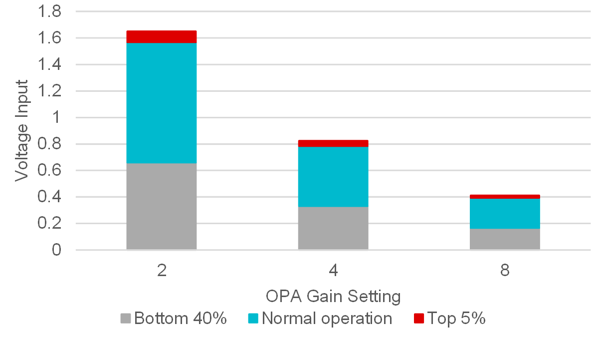
- The levels discussed in Design Steps 5 and 6 (HT is top 5%; LT is lower 40%), can be visualized in the chart below in relation to different OPA Gain settings. These
values were chosen to help maximize resolution at lower voltage level inputs, with some buffer for transitions. In the chart below, red corresponds to Design Step 5 transition level, gray represents Design Step 6 transition level, and
finally the blue area represents the voltage ranges where gain remains unchanged. More information about choosing your transition levels is discussed in Design Consideration 6.
- Setup OPA in SysConfig for PGA configuration with external input and external output.
- Setup ADC in SysConfig for window comparator mode with VCC as reference (VRef_ADC), sampling the OPA output.
- Convert the transition levels determined in Design Steps 5 and 6 to ADC codes using the equation from Design Step 3, and place these into the ADC window comparator limits in SysConfig.
- (Optionally) Setup ADC to also sample OPA output with chosen ADCMEMx.
- Set ADC sample time in SysConfig to a minimum time of tSample_PGA as given in the data sheet of the device.
Design Considerations
- OPA supply is the VCC of the MSPM0.
- OPA GBW setting: A lower GBW setting for the OPA consumes less current, but responds slower; conversely, a higher GBW consumes more current, but has a larger slew rate and faster enable and settling times. Please check device specific data sheet for exact specification differences between the modes
- OPA Gain transitions: If it is desired to skip OPA gain levels, additional code must be added to the ADC Window Comparator interrupt service routine (ISR) to explicitly set OPA gain settings, instead of just increasing or decreasing levels. Take care that your transition levels calculated in Design Steps 5 and 6 also reflect this type of transition.
- Minimum OPA Gain: The MSPM0 MCUs have the ability to dynamically change the OPA gain settings without disabling the OPA. The minimum gain for the OPA in a PGA configuration is 2. To change from a gain of 2 to an OPA Buffer configuration (OPA gain = 1), an additional procedure outside the scope of this document must be performed to reconfigure the OPA to this mode.
- ADC Reference selection: MSPM0 devices can provide a reference voltage to the ADC from the internal reference generator (VREF), an external source, or MCU VCC. Check your MSPM0 device data sheet for options available for your chosen device. The reference voltage chosen sets the full scale range the ADC can sample and must accommodate the maximum OPA output voltage
-
ADC Window Comparator levels:
- When increasing amplification of your input signal, by transitioning from a lower gain value to a higher gain value (Example: G = 2 -> 4), use the equation in Design Step 2 to determine if the voltage level chosen for transition does not rail the signal at the new gain setting.
- When decreasing amplification of your input signal, by transitioning from a higher gain value down to a lower gain value (Example: G = 4 -> 2), make sure that the voltage level chosen is greater than transition level chosen in Design Consideration 6.a. This is to avoid a loop of changing gain that can cause a system instability.
- ADC sampling: This example continuously samples the OPA output in window comparator mode. If continuous monitoring of the OPA output is not desired, a timer can be used to set a fixed interval of sampling.
- ADC results: The code example with optional ADC sampling of OPA output only stores the most current result captured in the global variable gADCResult . Full applications can store several readings in an array before performing actions on the data.
- ADC results: If using the option for capturing ADC results, code must be added to handle the data being processed in correlation to current OPA Gain settings. This because the ADC full-scale range changes in relation to OPA gain settings, and thus the same ADC codes can be seen at different input voltage levels of the OPA.
- Race conditions on gCheckADC: This application clears gCheckADC as soon as possible. If the application waits too long to clear gCheckADC it may inadvertently miss new data.
Software Flowchart
Figure 1-2 shows the code flow diagram for Dynamic_PGA_Example2 which explains how the ADC samples the OPA output and changes the OPA gain. The software flowchart for Dynamic_PGA1_Example is slightly simplified from the flow below, as the main loop goes to sleep after starting the ADC, and the center switch case for the ADC Interrupt Service Routine (ISR) is not present.
 Figure 1-2 Application Software Flowchart
Device Configuration
This application makes use of TI System Configuration Tool (SysConfig) graphical interface to generate the configuration code for the OPA and ADC. Using a graphical interface to configure the device peripherals streamlines the application prototyping process.
The code for what is described in Figure 2 can be found in the beginning of main() in the Dynamic_PGA1_Example.c or Dynamic_PGA_Example2.c files.
Application Code
The following code snippet shows where to adjust the OPA Gain levels and transition points as a relation of percentage of maximum ADC codes as described in Design Steps 2. See the MSPM0 SDK and DriverLib documentation for available OPA Gain defines.
#include "ti_msp_dl_config.h"

#define HIGHMARGIN 3890 // 4095*0.75 = 75% of max ADC value
#define LOWMARGIN  1638 // 4095*0.25 = 25% of max ADC value
#define MAXGAIN  DL_OPA_GAIN_N7_P8 // Maximum GAIN level of OPA wanted
#define MINGAIN  DL_OPA_GAIN_N1_P2 // Minimum GAIN level of OPA wanted.
//For non-inverting PGA mode this is an OPA GAIN of 2x. See advisory in TRM for MIN GAIN.
The following code snippet shows where to add custom code to perform useful actions after obtaining the ADC results. Typically this is some sort of math, placing multiple results in an array, filtering, or lookup table access.
    while (1) {
        //This while loop waits until the next ADC result is loaded
        while (false == gCheckADC) {
            __WFE();
        }
        gCheckADC = false;
        //Grab latest ADC Result
        gADCResult = DL_ADC12_getMemResult(ADC12_0_INST, DL_ADC12_MEM_IDX_0);

        //Add in code to do math on ADC results.
        //Scaling factors for the math will be dependent on the current OPA Gain levels.
    }
The following code snippet shows where to adjust the ADC result interpretation in relation to OPA Gain setting. It is up to the user to determine what actions to take, and how to correlate ADC results with OPA Gain setting and input voltage.
     switch (DL_ADC12_getPendingInterrupt(ADC12_0_INST)) {
        case DL_ADC12_IIDX_WINDOW_COMP_HIGH:
            // Entered high side margin window. Decrease OPA GAIN if possible.
            tempGain = DL_OPA_getGain(OPA_0_INST);
            if(tempGain > MINGAIN){
                //Update OPA gain.
                DL_OPA_decreaseGain(OPA_0_INST);
               //For full applications, at this point you would want to adjust any math factors or
               //look up tables to the new voltage ranges being captured by the ADC, or set a flag to do so in main while loop.
            }
            break;
        case DL_ADC12_IIDX_WINDOW_COMP_LOW:
            // Entered low side margin window. Increase OPA GAIN if possible.
            tempGain = DL_OPA_getGain(OPA_0_INST);
            if(tempGain < MAXGAIN){
               //Update OPA gain.
               DL_OPA_increaseGain(OPA_0_INST);
               //For full applications, at this point you would want to adjust any math factors or
               //look up tables to the new voltage ranges being captured by the ADC, or set a flag to do so in main while loop.
            }
            break;
        default:
            break;
    }
Results
The following graphs show captures of the OPA input changing and the corresponding gained output. The OPA Gain levels are as follows: 2x, 4x, 8x.
 Figure 1-3 Increasing OPA PGA Gain
 Figure 1-4 Decreasing OPA PGA Gain