SLAAEG1 February 2024 MSPM0L1306
Introduction
Electric vehicles are becoming more and more popular. On-board chargers (OBC) are important to charge the vehicle battery safely and smartly. Most of the time, OBC is in sleep mode. The OBC wakes up and functions after detecting signals from the charging gun. Based on the GB/T 18487.1-2015 standard, there are two types of required signals for AC charging gun detection. The CC signal determines the connection status between the OBC and the charging gun, and the CP signal determines the valid voltage and duty cycle status of the AC power supply.
To detect the CC and CP signals, determine the normal status, and wake up the host MCU to control the charging process, some designs leverage discrete designs with transistors, resistors and capacitors. However, it can be difficult to make changes for different project requirements and can require different PCB sizes. Now, a user can leverage a MSPM0 MCU to design a lower-power and higher-scalability integrated OBC wake-up design.
 Figure 1 OBC Charging Gun
Why build an integrated design with MSPM0?
- Low power: MSPM0 supports less than 1μA of standby current.
- High scalability: satisfies different requirements of wake-up delay time, condition, and source with flexible software design compared to fixed discrete hardware design.
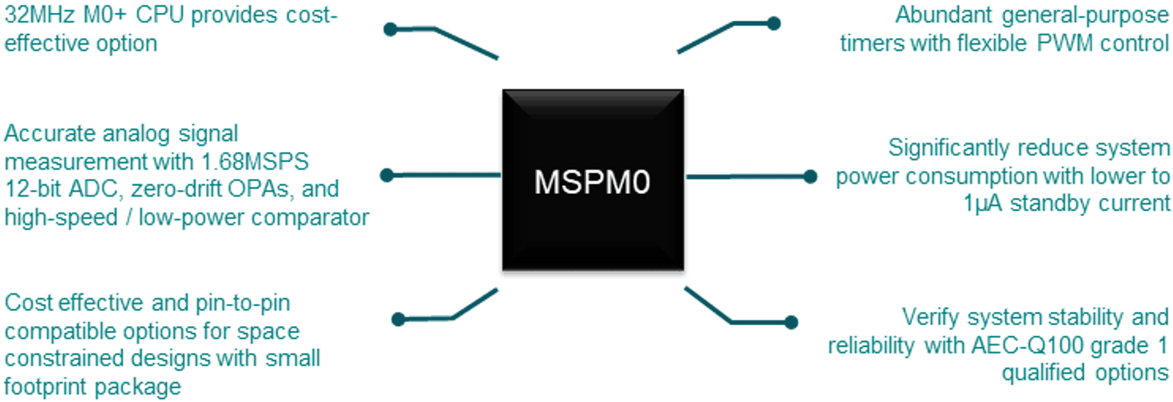
 Figure 2 MSPM0L Series Overview
What can MSPM0 do in an OBC wake-up design?
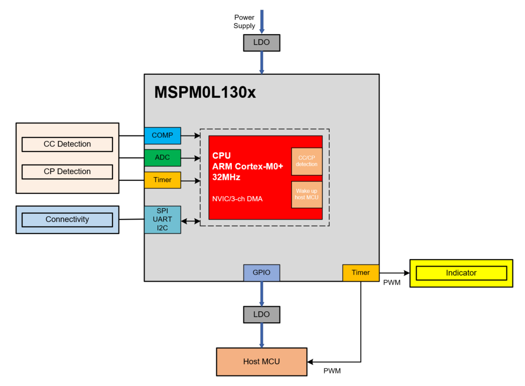
- Detect the resistance value of
the CC port to check the connection status between the OBC and the charging gun
by using an ADC or comparator module.
- 12-bit SAR ADC with 11.2ENOB and 1.68MSPS sampling rate.
- Two mode (low power and high speed) comparator with an 8-bit reference DAC.
- Detect the voltage and duty cycle
values of the CP port to find the valid wake-up status by using ADC and timer
modules.
- Four 16-bit timers that support low-power operation in standby mode.
- Enable the LDO for the host MCU and wake the MCU up to control the charging process by using a GPIO.
- More functions such as
controlling PWM indicators, and conducting protocol translations with multiple
enhanced communication interfaces.
- Two UART interfaces that support low-power operation in standby mode.
- Two I2C interfaces that support wakeup from stop mode.
- One SPI supports up to 16Mbit/s.
 Figure 3 Block Diagram of OBC Wake-up
Design Based on MSPM0L130x
Figure 3 Block Diagram of OBC Wake-up
Design Based on MSPM0L130xResources
Order a low-cost development kit LP-MSPM0L1306 to start designing an integrated OBC wake-up design. Jump-start coding with a MSPM0-SDK software development kit and the SysConfig graphical code generation tool. The following links show additional MSPM0 resources.
- Texas Instruments, MSPM0 overview page, product page.
- Texas Instruments, MSPM0L130x-Q1 Automotive Mixed-Signal Microcontrollers, data sheet.
- Texas Instruments, MSPM0 L-Series 32-MHz Microcontrollers Technical Reference Manual, technical reference manual.
- Texas Instruments, MSPM0 L-Series Hardware Development Guide, application note.
- Texas Instruments, MSPM0 Academy, training.