SLAU472C February 2013 – November 2023 TAS2505 , TAS2505-Q1
- 1
- Trademarks
- 1 TAS2505 Device Overview
- 2Description
-
3
TAS2505 Application
- 3.1 Terminal Descriptions
- 3.2 Audio Analog I/O
- 3.3 Analog Signals
- 3.4
Audio DAC and Audio Analog Outputs
- 3.4.1 DAC
- 3.4.2 DAC Gain Setting
- 3.4.3 Interrupts
- 3.4.4 Programming DAC Digital Filter Coefficients
- 3.4.5 Updating DAC Digital Filter Coefficients During PLAY
- 3.4.6 Digital Mixing and Routing
- 3.4.7 Analog Audio Routing
- 3.4.8 Analog Outputs
- 3.4.9 Audio Output-Stage Power Configurations
- 3.4.10 5V LDO
- 3.4.11 POR
- 3.4.12 DAC Setup
- 3.5
PowerTune
- 3.5.1 PowerTune Modes
- 3.5.2 DAC Power Consumption
- 3.5.3
Speaker output Power Consumption
- 3.5.3.1 Speaker output, Mono, 48 kHz, Highest Performance, DVDD = IOVDD = 1.8 V, AVDD = 1.8 V, SPKVDD = 3.6V
- 3.5.3.2 Speaker output, Mono, Lowest Power Consumption
- 3.5.3.3 Speaker output, Mono, 8 kHz, Highest Performance, DVDD = IOVDD = 1.8 V, AVDD = 1.8 V, SPKVDD = 3.6V
- 3.5.3.4 Speaker output, Mono, Lowest Power Consumption
- 3.5.4
Headphone output Power Consumption
- 3.5.4.1 Headphone output, Mono, 48 kHz, Highest Performance, DVDD = IOVDD = 1.8 V, AVDD = 1.8 V, SPKVDD = 3.6V
- 3.5.4.2 Headphone output, Mono, Lowest Power Consumption, DVDD = IOVDD = 1.8 V, AVDD = 1.5 V, SPKVDD = 3.6V
- 3.5.4.3 Headphone output, Mono, 8 kHz, Highest Performance, DVDD = IOVDD = 1.8 V, AVDD = 1.8 V, SPKVDD = 3.6V
- 3.5.4.4 Headphone output, Mono, Lowest Power Consumption, DVDD = IOVDD = 1.8 V, AVDD = 1.8 V, SPKVDD = 3.6V
- 3.6 CLOCK Generation and PLL
- 3.7 Digital Audio and Control Interface
- 3.8 Power Supply
- 3.9 Device Special Functions
- 4Device Initialization
-
5Example Setups
- 5.1 Example Register Setup to Play Digital Data Through DAC and Headphone/Speaker Outputs
- 5.2 Example Register Setup to Play Digital Data Through DAC and Headphone Output
- 5.3 Example Register Setup to Play AINL and AINR Through Headphone/Speaker Outputs
- 5.4 Example Register Setup to Play AINL and AINR Through Headphone Output
- 5.5 Example Register Setup to Play Digital Data Through DAC and Headphone/Speaker Outputs With 3 Programmable Biquads
- 5.6 Example Register Setup to Play Digital Data Through DAC and Headphone/Speaker Outputs With 6 Programmable Biquads
-
6Register Map
- 6.1
TAS2505 Register Map
- 6.1.1 Control Registers, Page 0 (Default Page): Clock Multipliers, Dividers, Serial Interfaces, Flags, Interrupts, and GPIOs
- 6.1.2 Control Registers, Page 1: DAC Routing, Power-Controls and MISC Logic Related Programmabilities
- 6.1.3 Page 2 - 43: Reserved Register
- 6.1.4 Page 44: DAC Programmable Coefficients RAM
- 6.1.5 Page 45 - 52: DAC Programmable Coefficients RAM
- 6.1.6 Page 53 - 61: Reserved Register
- 6.1.7 Page 62 - 70: DAC Programmable Coefficients RAM
- 6.1.8 Pages 71 – 255: Reserved Register
- 6.1.9 DAC Coefficients A+B
- 6.1.10 DAC Defaults
- 6.1
TAS2505 Register Map
- 7Revision History
3.6 CLOCK Generation and PLL
The TAS2505 supports a wide range of options for generating clocks for the DAC sections as well as interface and other control blocks as shown in . The clocks for the DAC require a source reference clock. This clock can be provided on a variety of device pins, such as the MCLK, BCLK, or GPIO pins. The source reference clock for the codec can be chosen by programming the CODEC_CLKIN value on page 0, register 4, bits D1–D0. The CODEC_CLKIN can then be routed through highly-flexible clock dividers shown in to generate the various clocks required for the DAC and the Digital Effects section. In the event that the desired audio clocks cannot be generated from the reference clocks on MCLK, BCLK, or GPIO, the TAS2505 also provides the option of using the on-chip PLL which supports a wide range of fractional multiplication values to generate the required clocks. Starting from CODEC_CLKIN, the TAS2505 provides several programmable clock dividers to help achieve a variety of sampling rates for the DAC and clocks for the Digital Effects sections.
 Figure 3-8 Clock Distribution Tree
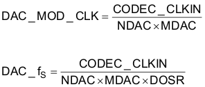
| Divider | Bits |
|---|---|
| NDAC | Page 0, register 11, bits D6–D0 |
| MDAC | Page 0, register 12, bits D6–D0 |
| DOSR | Page 0, register 13, bits D1–D0 and page 0, register 14, bits D7–D0 |
The DAC modulator is clocked by DAC_MOD_CLK. For proper power-up operation of the DAC channel, these clocks must be enabled by configuring the NDAC and MDAC clock dividers (page 0, register 11, bit D7 = 1 and page 0, register 12, bit D7 = 1). When the DAC channel is powered down, the device internally initiates a power-down sequence for proper shut-down. During this shutdown sequence, the NDAC and MDAC dividers must not be powered down, or else a proper low-power shutdown may not take place. The user can read back the power-status flag at page 0, register 37, bit D7 and page 0, register 37, bit D3. When both the flags indicate power-down, the MDAC divider may be powered down, followed by the NDAC divider.
In general, all the root clock dividers should be powered down only after the child clock dividers have been powered down for proper operation.
The TAS2505 also has options for routing some of the internal clocks to the GPIO output pin to be used as general-purpose clocks in the system. The feature is shown in Figure 3-10.
 Figure 3-9 BCLK Output Options
In the mode when TAS2505 is configured to drive the BCLK pin (page 0, register 27, bit D3 = 1), it can be driven as a divided value of BDIV_CLKIN. The division value can be programmed in page 0, register 30, bits D6–D0 from 1 to 128 (see Figure 3-9). The BDIV_CLKIN can itself be configured to be one of DAC_CLK (DAC DSP clock) or DAC_MOD_CLK by configuring the BDIV_CLKIN multiplexer in page 0, register 29, bits D1-D0. Additionally, a general-purpose clock can be driven out on GPIO.
This clock can be a divided-down version of CDIV_CLKIN. The value of this clock divider can be programmed from 1 to 128 by writing to page 0, register 26, bits D6–D0. The CDIV_CLKIN can itself be programmed as one of the clocks among the list shown in Figure 3-10. This can be controlled by programming the multiplexer in page 0, register 25, bits D2–D0.
 Figure 3-10 General-Purpose Clock Output Options
| Clock | DVDD ≥ 1.65 V |
|---|---|
| CODEC_CLKIN | ≤ 110 MHz |
| DAC_CLK | ≤ 49.152 MHz |
| DAC_MOD_CLK | 6.758 MHz |
| DAC_fS | 0.192 MHz |
| BDIV_CLKIN | 55 MHz |
| CDIV_CLKIN | 100 MHz when M is odd 110 MHz when M is even |