SLAU472C February   2013  – November 2023 TAS2505 , TAS2505-Q1


  1.   1
  2.   Trademarks
  3. 1 TAS2505 Device Overview
  4. 2Description
    1. 2.1 Typical Circuit Configuration
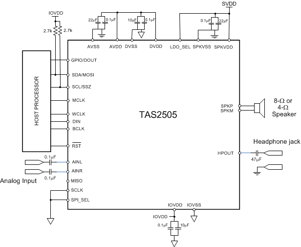
    2. 2.2 Circuit Configuration with Internal LDO
  5. 3 TAS2505 Application
    1. 3.1 Terminal Descriptions
      1. 3.1.1 Digital Pins
      2. 3.1.2 Analog Pins
      3. 3.1.3 Multifunction Pins
      4. 3.1.4 Register Settings for Multifunction Pins
    2. 3.2 Audio Analog I/O
    3. 3.3 Analog Signals
      1. 3.3.1 Analog Inputs AINL and AINR
    4. 3.4 Audio DAC and Audio Analog Outputs
      1. 3.4.1  DAC
        1. 3.4.1.1 DAC Processing Blocks
        2. 3.4.1.2 DAC Processing Blocks – Signal Chain Details
          1. 3.4.1.2.1 Three Biquads, Filter A
          2. 3.4.1.2.2 Six Biquads, First-Order IIR, Filter A or B
        3. 3.4.1.3 DAC User-Programmable Filters
          1. 3.4.1.3.1 First-Order IIR Section
          2. 3.4.1.3.2 Biquad Section
        4. 3.4.1.4 DAC Interpolation Filter Characteristics
          1. 3.4.1.4.1 Interpolation Filter A
          2. 3.4.1.4.2 Interpolation Filter B
      2. 3.4.2  DAC Gain Setting
        1. 3.4.2.1 PowerTune Modes
        2. 3.4.2.2 DAC Digital-Volume Control
      3. 3.4.3  Interrupts
      4. 3.4.4  Programming DAC Digital Filter Coefficients
      5. 3.4.5  Updating DAC Digital Filter Coefficients During PLAY
      6. 3.4.6  Digital Mixing and Routing
      7. 3.4.7  Analog Audio Routing
        1. 3.4.7.1 Analog Output Volume Control
        2. 3.4.7.2 Headphone Analog Output Volume Control
        3. 3.4.7.3 Class-D Speaker Analog Output Volume Control
      8. 3.4.8  Analog Outputs
        1. 3.4.8.1 Headphone Drivers
        2. 3.4.8.2 Speaker Driver
      9. 3.4.9  Audio Output-Stage Power Configurations
      10. 3.4.10 5V LDO
      11. 3.4.11 POR
      12. 3.4.12 DAC Setup
    5. 3.5 PowerTune
      1. 3.5.1 PowerTune Modes
        1. 3.5.1.1 DAC - Programming PTM_P1 to PTM_P4
        2. 3.5.1.2 Processing Blocks
      2. 3.5.2 DAC Power Consumption
        1. 3.5.2.1 DAC, Mono, 48 kHz, Highest Performance, DVDD = IOVDD = 1.8 V, AVDD = 1.8 V, SPKVDD = 3.6V
        2. 3.5.2.2 DAC, Mono, Lowest Power Consumption
        3. 3.5.2.3 DAC, Mono, 8 kHz, Highest Performance, DVDD = IOVDD = 1.8 V, AVDD = 1.8 V, SPKVDD = 3.6 V
        4. 3.5.2.4 DAC, Mono, Lowest Power Consumption
      3. 3.5.3 Speaker output Power Consumption
        1. 3.5.3.1 Speaker output, Mono, 48 kHz, Highest Performance, DVDD = IOVDD = 1.8 V, AVDD = 1.8 V, SPKVDD = 3.6V
        2. 3.5.3.2 Speaker output, Mono, Lowest Power Consumption
        3. 3.5.3.3 Speaker output, Mono, 8 kHz, Highest Performance, DVDD = IOVDD = 1.8 V, AVDD = 1.8 V, SPKVDD = 3.6V
        4. 3.5.3.4 Speaker output, Mono, Lowest Power Consumption
      4. 3.5.4 Headphone output Power Consumption
        1. 3.5.4.1 Headphone output, Mono, 48 kHz, Highest Performance, DVDD = IOVDD = 1.8 V, AVDD = 1.8 V, SPKVDD = 3.6V
        2. 3.5.4.2 Headphone output, Mono, Lowest Power Consumption, DVDD = IOVDD = 1.8 V, AVDD = 1.5 V, SPKVDD = 3.6V
        3. 3.5.4.3 Headphone output, Mono, 8 kHz, Highest Performance, DVDD = IOVDD = 1.8 V, AVDD = 1.8 V, SPKVDD = 3.6V
        4. 3.5.4.4 Headphone output, Mono, Lowest Power Consumption, DVDD = IOVDD = 1.8 V, AVDD = 1.8 V, SPKVDD = 3.6V
    6. 3.6 CLOCK Generation and PLL
      1. 3.6.1 PLL
        1. 3.6.1.1 PLL Description
    7. 3.7 Digital Audio and Control Interface
      1. 3.7.1 Digital Audio Interface
        1. 3.7.1.1 Right-Justified Mode
        2. 3.7.1.2 Left-Justified Mode
        3. 3.7.1.3 I2S Mode
        4. 3.7.1.4 DSP Mode
        5. 3.7.1.5 Primary and Secondary Digital Audio Interface Selection
      2. 3.7.2 Control Interface
        1. 3.7.2.1 I2C Control Mode
        2. 3.7.2.2 SPI Digital Interface
    8. 3.8 Power Supply
      1. 3.8.1 System Level Considerations
        1. 3.8.1.1 All Supplies from Single Voltage Rail with using the internal LDO (2.75V to 5.5V)
          1. 3.8.1.1.1 Standby Mode
          2. 3.8.1.1.2 Shutdown Mode
        2. 3.8.1.2 Supply from Dual Voltage Rails (2.75V to 5.5V and 1.8V)
          1. 3.8.1.2.1 Standby Mode
          2. 3.8.1.2.2 Shutdown Mode
        3. 3.8.1.3 Other Supply Options
    9. 3.9 Device Special Functions
      1. 3.9.1 Interrupts
  6. 4Device Initialization
    1. 4.1 Power On Sequence
      1. 4.1.1 Power On Sequence 1 – Separate Digital and Analog Supplies
      2. 4.1.2 Power On Sequence 2 – Shared 1.8 V Analog Supply to DVDD
    2. 4.2 Device Initialization
      1. 4.2.1 Reset by RST pin and POR
      2. 4.2.2 Device Start-Up Lockout Times
      3. 4.2.3 PLL Start-Up
      4. 4.2.4 Power-Stage Reset
      5. 4.2.5 Software Power Down
      6. 4.2.6 Device Common Mode Voltage
  7. 5Example Setups
    1. 5.1 Example Register Setup to Play Digital Data Through DAC and Headphone/Speaker Outputs
    2. 5.2 Example Register Setup to Play Digital Data Through DAC and Headphone Output
    3. 5.3 Example Register Setup to Play AINL and AINR Through Headphone/Speaker Outputs
    4. 5.4 Example Register Setup to Play AINL and AINR Through Headphone Output
    5. 5.5 Example Register Setup to Play Digital Data Through DAC and Headphone/Speaker Outputs With 3 Programmable Biquads
    6. 5.6 Example Register Setup to Play Digital Data Through DAC and Headphone/Speaker Outputs With 6 Programmable Biquads
  8. 6Register Map
    1. 6.1 TAS2505 Register Map
      1. 6.1.1  Control Registers, Page 0 (Default Page): Clock Multipliers, Dividers, Serial Interfaces, Flags, Interrupts, and GPIOs
      2. 6.1.2  Control Registers, Page 1: DAC Routing, Power-Controls and MISC Logic Related Programmabilities
      3. 6.1.3  Page 2 - 43: Reserved Register
      4. 6.1.4  Page 44: DAC Programmable Coefficients RAM
      5. 6.1.5  Page 45 - 52: DAC Programmable Coefficients RAM
      6. 6.1.6  Page 53 - 61: Reserved Register
      7. 6.1.7  Page 62 - 70: DAC Programmable Coefficients RAM
      8. 6.1.8  Pages 71 – 255: Reserved Register
      9. 6.1.9  DAC Coefficients A+B
      10. 6.1.10 DAC Defaults
  9. 7Revision History

Circuit Configuration with Internal LDO

GUID-63ADB419-6758-4A58-B582-067BBB257026-low.gifFigure 2-3 Application Schematics for LDO