SLAZ186T October 2012 – May 2021 MSP430F2616
- 1Functional Advisories
- 2Preprogrammed Software Advisories
- 3Debug Only Advisories
- 4Fixed by Compiler Advisories
- 5Nomenclature, Package Symbolization, and Revision Identification
-
6Advisory Descriptions
- 6.1 ADC25
- 6.2 BCL12
- 6.3 BCL13
- 6.4 BCL15
- 6.5 CPU8
- 6.6 CPU16
- 6.7 CPU19
- 6.8 DAC4
- 6.9 DMA3
- 6.10 DMA4
- 6.11 DMA13
- 6.12 FLASH19
- 6.13 FLASH24
- 6.14 FLASH25
- 6.15 FLASH27
- 6.16 FLASH36
- 6.17 JTAG23
- 6.18 PORT10
- 6.19 PORT12
- 6.20 TA12
- 6.21 TA16
- 6.22 TA21
- 6.23 TAB22
- 6.24 TB2
- 6.25 TB16
- 6.26 TB24
- 6.27 USCI20
- 6.28 USCI21
- 6.29 USCI22
- 6.30 USCI23
- 6.31 USCI24
- 6.32 USCI25
- 6.33 USCI26
- 6.34 USCI27
- 6.35 USCI30
- 6.36 USCI34
- 6.37 USCI35
- 6.38 USCI40
- 6.39 XOSC5
- 6.40 XOSC8
- 7Revision History
6.2 BCL12
BCL Module
Category
Functional
Function
Switching RSELx or modifying DCOCTL can cause DCO dead time or a complete DCO stop
Description
After switching RSELx bits (located in register BCSCTL1) from a value of >13 to a value of <12 OR from a value of <12 to a value of >13, the resulting clock delivered by the DCO can stop before the new clock frequency is applied. This dead time is approximately 20 us. In some instances, the DCO may completely stop, requiring a power cycle.
Furthermore, if all of the RSELx bits in the BSCTL1 register are set, modifying the DCOCTL register to change the DCOx or the MODx bits could also result in DCO dead time or DCO hang up.
Workaround
- When switching RSEL from >13 to <12, use an intermediate frequency step. The intermediate RSEL value should be 13.
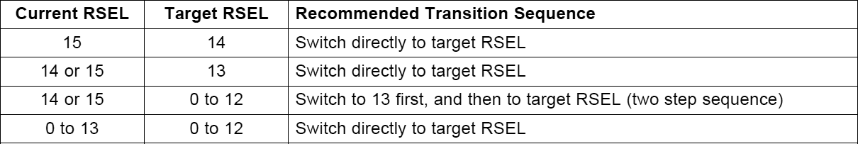
AND
- When switching RSEL from <12 to >13 it's recommended to set RSEL to its default value first (RSEL = 7) before switching to the desired target frequency.
AND
- In case RSEL is at 15 (highest setting) it's recommended to set RSEL to its default value first (RSEL = 7) before accessing DCOCTL to modify the DCOx and MODx bits. After the DCOCTL register modification the RSEL bits can be manipulated in an additional step.
In the majority of cases switching directly to intermediate RSEL steps as described above will prevent the occurrence of BCL12. However, a more reliable method can be implemented by changing the RSEL bits step by step in order to guarantee safe function without any dead time of the DCO.
Note that the 3-step clock startup sequence consisting of clearing DCOCTL, loading the BCSCTL1 target value, and finally loading the DCOCTL target value as suggested in the in the "TLV Structure" chapter of the MSP430x2xx Family User's Guide is not affected by BCL12 if (and only if) it is executed after a device reset (PUC) prior to any other modifications being made to BCSCTL1 since in this case RSEL still is at its default value of 7. However any further changes to the DCOx and MODx bits will require the consideration of the workaround outlined above.