SLLU265C March 2018 – April 2024 TUSB1044
2.2.1 TUSB1044 EVM Default Jumper and Switch Configuration
The following headers are provided for TUSB1044 configuration by default, configuration settings need to be optimized depending on the amount of loss of each channel in the system.
Table 2-1 TUSB1044 Configuration
Pins
| Reference Designator |
JMP Control | Configuration |
|---|---|---|
| J1 | CTL0/SDA | No Connect |
| J2 | FLIP/SCL | No Connect |
| J3 | HPDIN | No Connect |
| J4 | VCC Isolate | No Connect |
| J6 | VCC33 | No Connect |
| J9 | 1044_IO | SHUNT on pin 1-2 (2P5) |
| JMP2 | DEQ1 | SHUNT on pin 1-2 (GND) |
| JMP3 | DEQ0 | SHUNT on pin 1-2 (GND) |
| JMP4 | UEQ1/A1 | SHUNT on pin 1-2 (GND) |
| JMP5 | UEQ0/A0 | SHUNT on pin 1-2 (GND) |
| JMP6 | CFG1 | SHUNT on pin 2–4 (20K PD) |
| JMP7 | CFG0 | SHUNT on pin 1-2 (GND) |
| JMP8 | VIO_SEL | SHUNT on pin 1-2 (GND) |
| JMP9 | I2C_EN | SHUNT on pin 1-2 (GND) |
| JMP10 | EQ1 | SHUNT on pin 1-2 (200Ω to GND) |
| JMP11 | DC_BOOST1 | SHUNT on pin 1-2 (20kΩ to 3.3V) |
| JMP12 | EQ2 | SHUNT on pin 1-2 (200Ω to GND) |
| JMP13 | DC_BOOST2 | SHUNT on pin 1-2 (20kΩ to 3.3V) |
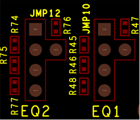
Note: Figure 3-3 and Figure 3-4 show how some early boards were built with a different configuration of JMP10 and
JMP12. For these boards, connect a jumper wire from pin 1 to pins 3–5.
 Figure 2-3 Early Board JMP10 and JMP12 Schematic
 Figure 2-4 Early
Board JMP10 and JMP12 Layout
Figure 2-4 Early
Board JMP10 and JMP12 LayoutTable 2-2 Switch Configuration
| SW1 Position | Control Signal | Configuration |
|---|---|---|
| 1 | EN | ON |
| 2 | SWAP | OFF |
| 3 | SLP_S0# | ON |
| 4 | DIR1 | OFF |
| 5 | DIR0 | OFF |
| 6 | CTL1 | ON |
| 7 | CTL0/SDA | ON |
| 8 | FLIP/SCL | OFF |