SLLU312A July 2019 – May 2022 TCAN4550-Q1
- TCAN4550-Q1 Functional Safety-Manual
- Trademarks
- 1Introduction
- 2Product Functional Safety-Capability
- 3Product Overview
- 4Development Process for Management of Systematic Faults
- 5Revision History
3 Product Overview
The TCAN4550-Q1 is a CAN FD controller with an integrated CAN FD transceiver supporting data rates up to 8 Mbps. The CAN FD controller meets the specifications of the ISO 11898-1:2015 high speed Controller Area Network (CAN) data link layer and meets the physical layer requirements of the ISO 11898-2:2016 High Speed Controller Area Network (CAN) specification providing an interface between the CAN bus and the host system supporting both classical CAN and CAN FD up to 8 megabits per second (Mbps). The TCAN4550-Q1 provides CAN FD transceiver functionality: differential transmit capability to the bus and differential receive capability from the bus. The device includes many protection features providing device and CAN bus robustness. The device can also wake up via remote wake up using the CAN bus implementing the ISO 11898-2:2016 Wake Up Pattern (WUP). Input/Output support for 3.3 V and 5 V microprocessors using the VIO pin for a seamless interface. The TCAN4550-Q1 has a Serial Peripheral Interface (SPI) that connects to a local microprocessor for the device configuration, transmission and reception of CAN frames. The SPI interface supports clock rates up to 18 MHz.
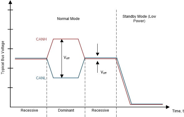
The CAN bus has two logical states during operation: recessive and dominant. See Figure 3-1
In the recessive bus state, the bus is biased to a common mode of about 2.5 V via the high resistance internal input resistors of the receiver of each node. Recessive is equivalent to logic high and is typically a differential voltage on the bus of almost 0 V. The recessive state is also the idle state.
In the dominant bus state, the bus is driven differentially by one or more drivers. Current flows through the termination resistors and generates a differential voltage on the bus. Dominant is equivalent to logic low and is a differential voltage on the bus greater than the minimum threshold for a CAN dominant. A dominant state overwrites the recessive state.
During arbitration, multiple CAN nodes may transmit a dominant bit at the same time. In this case the differential voltage of the bus may be greater than the differential voltage of a single driver.
Transceivers with low power Standby Mode have a third bus state where the bus terminals are weakly biased to ground via the high resistance internal resistors of the receiver. See Figure 3-1 and Figure 3-2.
Many of the pins can be configured for multiple purposes. Much of the parametric data is based on internal links like the TXD/RXD_INT which represent the TXD and RXD of a standalone CAN transceiver. The TCAN4550-Q1 has a test mode that maps these signals to an external pin in order to perform compliance testing on the transceiver (TXD/RXD_INT_PHY) and CAN controller (TXD/RXD_INT_CAN) independently.
 Figure 3-1 CAN Bus States