SLLU337 June 2021 ISOW1432
4 EVM 3D Diagram and PCB Layout
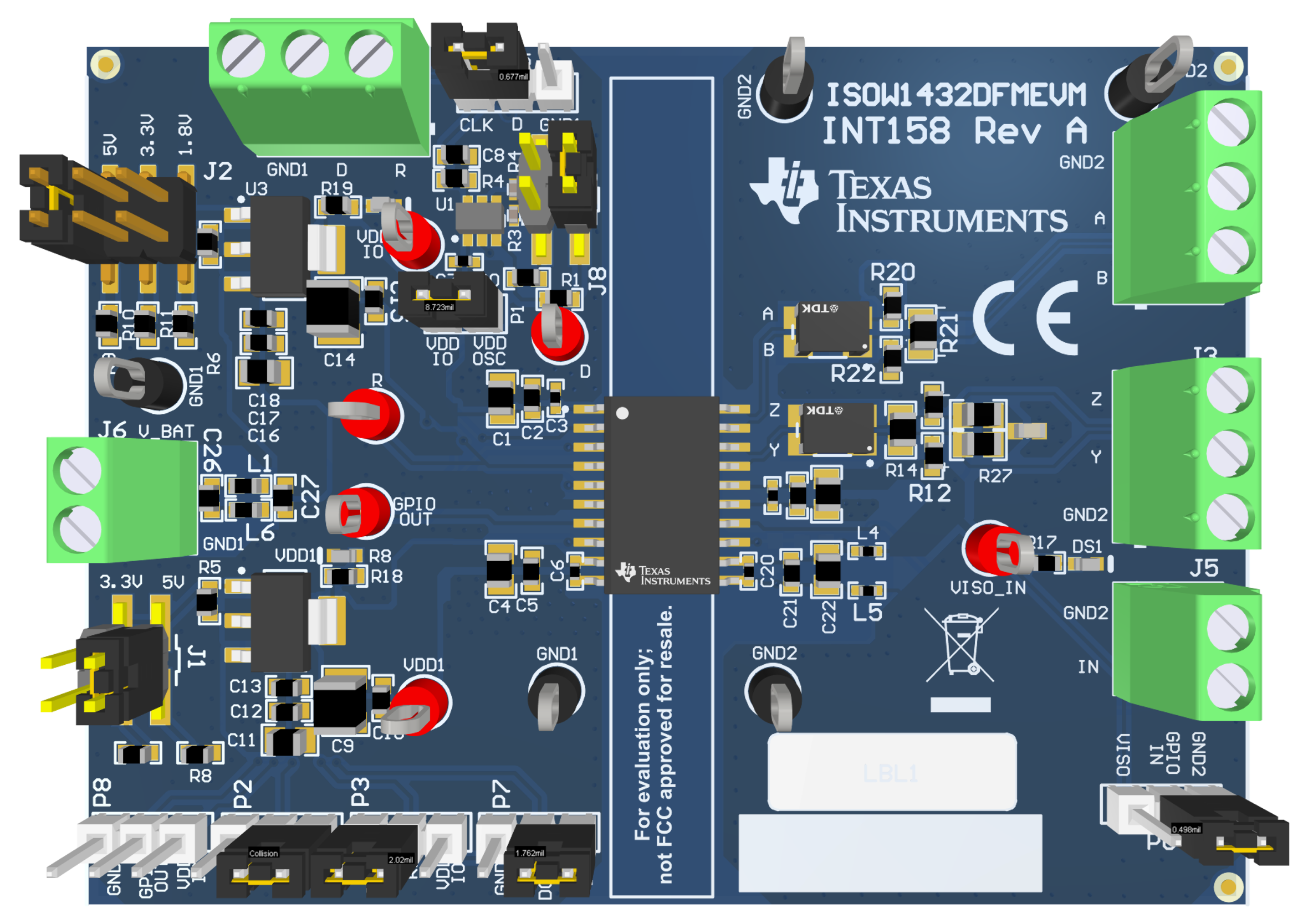
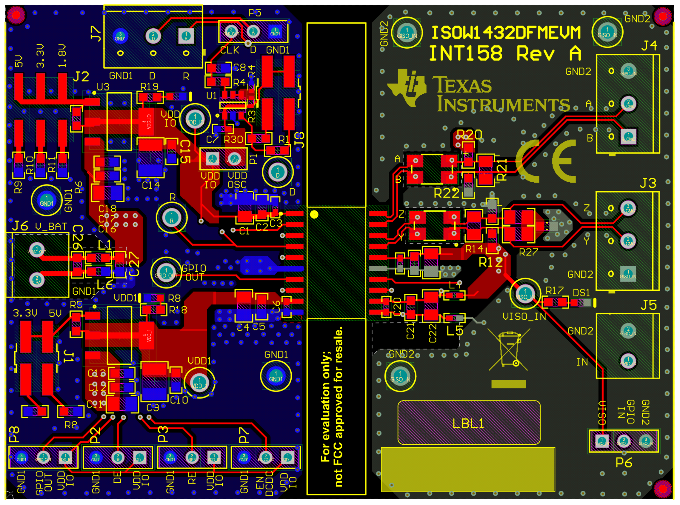
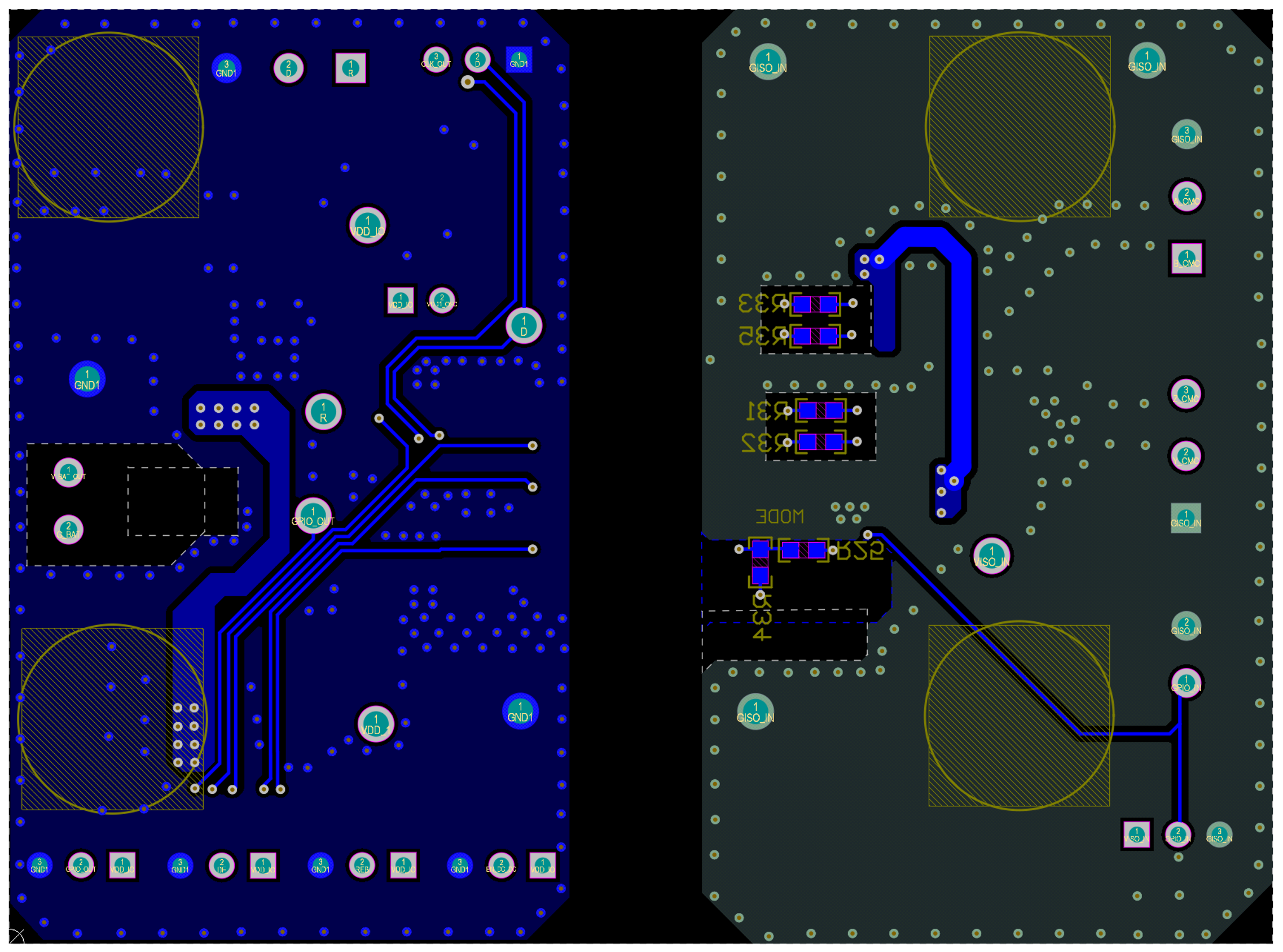
Figure 4-1 shows 3D diagram of ISOW1432DFMEVM. Figure 4-2 and Figure 4-3 show the PCB layout of ISOW1432DFMEVM, respectively.
 Figure 4-1 ISOW1432DFMEVM PCB 3D
diagram
 Figure 4-2 ISOW1432DFMEVM PCB Layout -
Top Layer
 Figure 4-3 ISOW1432DFMEVM PCB Layout -
Bottom Layer