SLUA669B March 2013 – September 2023 UCC27511 , UCC27531 , UCC27532 , UCC27533 , UCC27536 , UCC27537 , UCC27538
2.2 Bootstrap Bias Supply with Capacitive Signal Isolation Solution
Signal Isolation
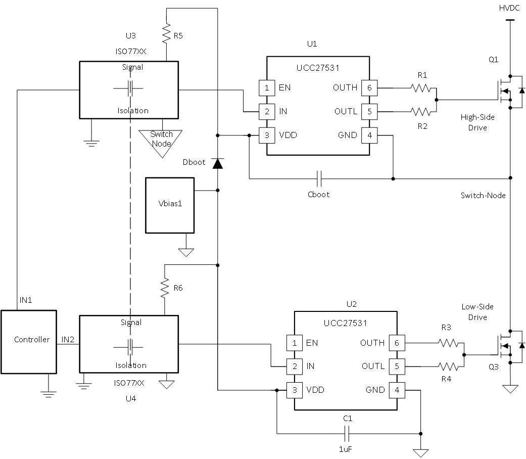
 Figure 2-2 High-Side Bootstrap Circuit Using Capacitor-Based Signal Isolation
In Figure 2-2, the input to U1 is isolated using U3. U3 is capacitive signal isolator ISO77xx. Capacitive-based isolators can signal properly even with large common-mode ground slew-rates, they are more stable over life and temperature compared to optocouplers, and they do not have the duty cycle limitations of gate-drive transformers.
High-Side Bias
In Figure 2-2, Dboot and Cboot are used as a bootstrap circuit to bias U1 properly when Q1 is turned on. When Q1 is off, Dboot is forward biased and U1 is supplied directly from Vbias1 while Cboot is charged. When Q1 turns on, the switch-node voltage increases to HVDC, Dboot is reverse-biased and protecting Vbias1, and U1 is powered as Cboot empties its charge into the VDD pin of U1. This charge from Cboot must be adequate to keep U1 on throughout the entire time that Q1 is on. Sizing of Dboot and Cboot are beyond the scope of this article. In the UCC27712 datasheet, refer to for selecting Cboot and for selecting Dboot.