SLUAA81A October 2020 – February 2022 BQ769142 , BQ76922 , BQ76942 , BQ76952
2.4 External Cell-Balancing Circuit Design Using BJTs
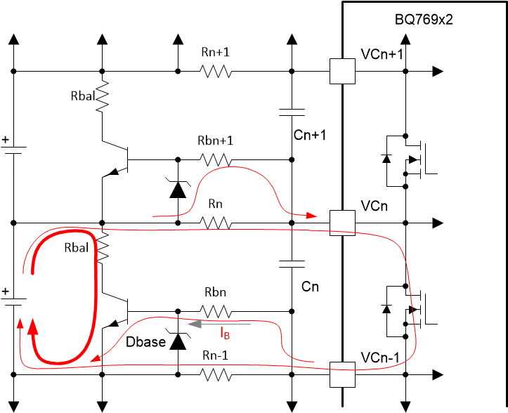
External FETs work well for most applications with typical 4.2 V lithium ion cells since balancing is most commonly done at higher voltages during charge. For applications that need higher balancing current than the internal balancing can provide but also need to balance at lower cell voltages, external BJTs may be considered. The balancing current for an external BJT can be controlled by selecting the appropriate balance resistor (Rbal) and base resistor (Rbn). In Figure 2-5, as the internal FET is turned on inside the device, the current flowing through Rbn puts the NPN transistor into saturation.
 Figure 2-5 Balancing Circuit Using External
BJTs
Figure 2-5 Balancing Circuit Using External
BJTsA Zener diode is also used in this circuit to protect from pack transients similar to the FET circuits. A standard diode is also suitable to use instead of a Zener when using BJTs because it is the forward voltage of the Zener that protects the transistor. The base-emitter diode (or emitter-base diode for a PNP) will conduct in the reverse direction which will prevent the Zener from conducting.
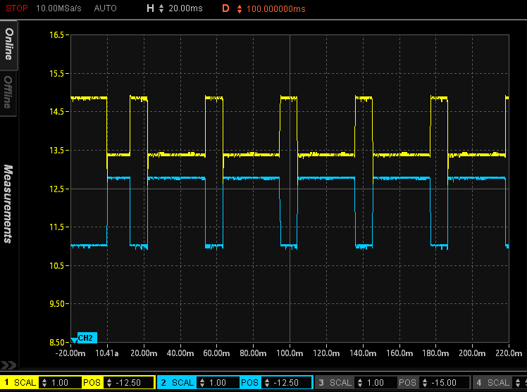
For the waveform captured below, the circuit was designed with an Rn of 100 Ω and Rgn of 240 Ω. The Rbal resistor is set to 50 Ω for a balance current of 80 mA through the BJT at 4 V. At this cell voltage, an additional ~22 mA of current flows through the internal FET of the device for a total balancing current of close to 102 mA. An NPN transistor was selected with hFE of 30 at IC = 100 mA. With this component selection, IB is approximately 4.5 mA when the cell voltage is 4 V.
 Figure 2-6 BQ76942 Cell Balancing With NPN BJT,
Cell 4 (yellow) = 3.8 V, Cell 3 (blue) = 3.7 V