SLUS774C AUGUST 2007 – December 2014
PRODUCTION DATA.
- 1 Features
- 2 Applications
- 3 Description
- 4 Revision History
- 5 Pin Configuration and Functions
- 6 Specifications
-
7 Detailed Description
- 7.1 Overview
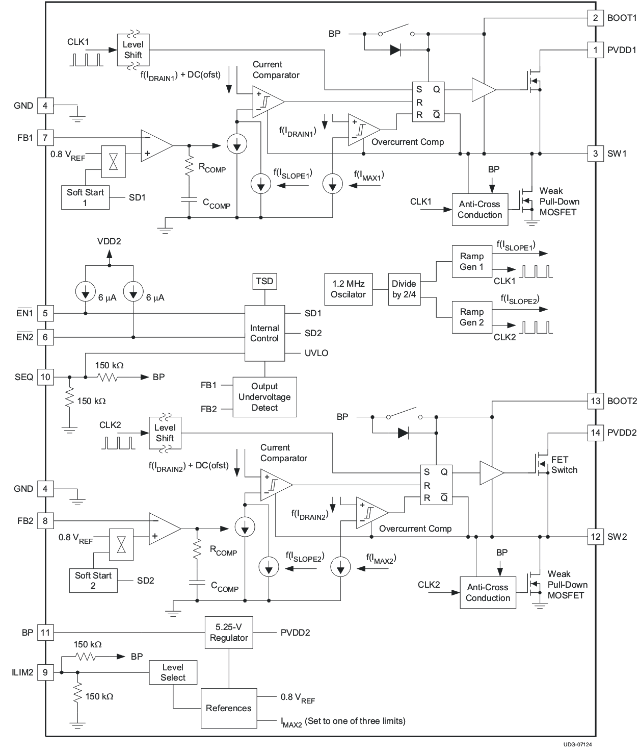
- 7.2 Functional Block Diagram
- 7.3
Feature Description
- 7.3.1 Voltage Reference
- 7.3.2 Oscillator
- 7.3.3 Input Undervoltage Lockout (UVLO) and Startup
- 7.3.4 Enable and Timed Turn On of the Outputs
- 7.3.5 Output Voltage Sequencing
- 7.3.6 Soft-Start
- 7.3.7 Output Voltage Regulation
- 7.3.8 Feedback Loop and Inductor-Capacitor (L-C) Filter Selection
- 7.3.9 Inductor-Capacitor (L-C) Selection
- 7.3.10 Maximum Output Capacitance
- 7.3.11 Minimum Output Capacitance
- 7.3.12 Modifying The Feedback Loop
- 7.3.13 Example: TPS54386 Buck Converter Operating at 12-V Input, 3.3-V Output and 400-mA(P-P) Ripple Current
- 7.3.14 Bootstrap for the N-Channel MOSFET
- 7.3.15 Light Load Operation
- 7.3.16 SW Node Ringing
- 7.3.17 Output Overload Protection
- 7.3.18 Operating Near Maximum Duty Cycle
- 7.3.19 Dual Supply Operation
- 7.3.20 Cascading Supply Operation
- 7.3.21 Multiphase Operation
- 7.3.22 Bypass and FIltering
- 7.3.23 Overtemperature Protection and Junction Temperature Rise
- 7.3.24 Power Derating
- 7.4 Device Functional Modes
-
8 Applications and Implementation
- 8.1 Application Information
- 8.2
Typical Applications
- 8.2.1
12-V to 5-V and 3.3-V Converter
- 8.2.1.1 Design Requirements
- 8.2.1.2
Detailed Design Procedure
- 8.2.1.2.1 Duty Cycle Estimation
- 8.2.1.2.2 Inductor Selection
- 8.2.1.2.3 Rectifier Diode Selection
- 8.2.1.2.4 Output Capacitor Selection
- 8.2.1.2.5 Voltage Setting
- 8.2.1.2.6 Compensation Capacitors
- 8.2.1.2.7 Input Capacitor Selection
- 8.2.1.2.8 Boot Strap Capacitor
- 8.2.1.2.9 ILIM
- 8.2.1.2.10 SEQ
- 8.2.1.2.11 Power Dissipation
- 8.2.1.3 Application Curves
- 8.2.2 24-V to 12-V and 24-V to 5-V
- 8.2.3 5-V to 3.3V and 5-V to 1.2 V
- 8.2.1
12-V to 5-V and 3.3-V Converter
- 9 Power Supply Recommendations
- 10Layout
- 11Device and Documentation Support
- 12Mechanical, Packaging, and Orderable Information
7 Detailed Description
7.1 Overview
The TPS54383 and TPS54386 are dual output, non-synchronous step down (buck) converters. Integrated into each PWM channel is an internally-compensated error amplifier, current mode pulse width modulator (PWM), switch MOSFET, internal bootstrap switch for high-side gate drive, and fault protection circuitry. Each channel also contains an EN pin and internal fixed soft-start time. The fault protection circuitry includes cycle-by-cycle current limit, output undervoltage detection, hiccup timeout and thermal shutdown. Channel 1 has a fixed current limit and channel 2 has three selectable overcurrent levels. Common to the two channels is the internal BP voltage regulator, voltage reference, clock oscillator, and output voltage sequencing functions.
DESIGN HINT
The TPS5438x contains internal slope compensation and loop compensation components; therefore, the external L-C filter must be selected appropriately so that the resulting control loop meets criteria for stability. This approach differs from an externally-compensated controller, where the L-C filter is generally selected first, and the compensation network is found afterwards. (See Feedback Loop and L-C Filter Selection section.)
NOTE
Unless otherwise noted, the term TPS5438x applies to both the TPS54383 and TPS54386. Also, unless otherwise noted, a label with a lowercase x appended implies the term applies to both outputs of the two modulator channels. For example, the term ENx implies both EN1 and EN2. Unless otherwise noted, all parametric values given are typical. Refer to the Electrical Characteristics for minimum and maximum values. Calculations should be performed with tolerance values taken into consideration.
7.2 Functional Block Diagram
7.3 Feature Description
7.3.1 Voltage Reference
The bandgap cell common to both outputs, trimmed to 800 mV.
7.3.2 Oscillator
The oscillator frequency is internally fixed at two times the SWx node switching frequency. The two outputs are internally configured to operate on alternating switch cycles (that is, 180° out of phase).
7.3.3 Input Undervoltage Lockout (UVLO) and Startup
When the voltage at the PVDD2 pin is less than 4.1 V, a portion of the internal bias circuitry is operational, and all other functions are held OFF. All of the internal MOSFETs are also held OFF. When the PVDD2 voltage rises above the UVLO turn-on threshold, the state of the enable pins determines the remainder of the internal startup sequence. If either output is enabled (ENx pulled low), the BP regulator turns on, charging the BP capacitor with a 20-mA current. When the BP pin is greater than 4 V, PWM is enabled and soft-start begins, depending on the SEQ mode of operation and the EN1 and EN2 settings.
Note that the internal regulator and control circuitry are powered from PVDD2. The voltage on PVDD1 may be higher or lower than PVDD2. (See the Dual Supply Operation section.)
7.3.4 Enable and Timed Turn On of the Outputs
Each output has a dedicated (active low) enable pin. If left floating, an internal current source pulls the pin to PVDD2. By grounding, or by pulling the ENx pin to below approximately 1.2 V with an external circuit, the associated output is enabled and soft-start is initiated.
If both enable pins are left in the high state, the device operates in a shutdown mode, where the BP regulator is shut down and minimal functions are active. The total standby current from both PVDD pins is approximately 70 μA at 12-V input supply.
An R-C connected to an ENx pin may be used to delay the turn-on of the associated output after power is applied to PVDDx (see Figure 16). After power is applied to PVDD2, the voltage on the ENx pin slowly decays towards ground. Once the voltage decays to approximately 1.2 V, then the output is enabled and the startup sequence begins. If it is desired to enable the outputs of the device immediately upon the application of power to PVDD2, then omit these two components and tie the ENx pin to GND directly.
If an R-C circuit is used to delay the turn-on of the output, the resistor value must be much less than 1.2 V / 6μA or 200 kΩ. A suggested value is 51 kΩ. This resistor value allows the ENx voltage to decay below the 1.2-V threshold while the 6-μA bias current flows.
The capacitor value required to delay the startup time (after the application of PVDD2) is shown in Equation 1.
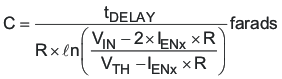
where
- R and C are the timing components
- VTH is the 1.2-V enable threshold voltage
- IENx is the 6 μA enable pin biasing current
Other enable pin functionality is dictated by the state of the SEQ pin. (See the Output Voltage Sequencing section.)
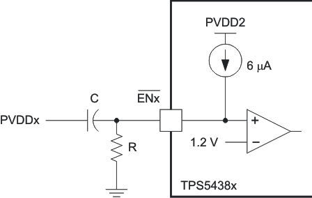 Figure 16. Startup Delay Schematic
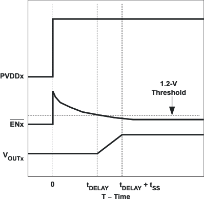 Figure 17. Startup Delay with R-C on Enable
DESIGN HINT
If delayed output voltage startup is not necessary, simply connect EN1 and EN2 to GND. This configuration allows the outputs to start immediately on valid application of PVDD2.
If ENx is allowed to go high after the Outputx has been in regulation, the upper MOSFET shuts off, and the output decays at a rate determined by the output capacitor and the load. The internal pulldown MOSFET remains in the OFF state. (See the Bootstrap for N-Channel MOSFET section.)
7.3.5 Output Voltage Sequencing
The TPS5438x allows single-pin programming of output voltage startup sequencing. During power-on, the state of the SEQ pin is detected. Based on whether the pin is tied to BP, to GND, or left floating, the outputs behave as described in Table 1.
Table 1. Sequence States
| SEQ PIN STATE | MODE | EN1 | EN2 |
|---|---|---|---|
| BP | Sequential, Output 2 then Output 1 | Ignored by the device.when VEN2 < enable threshold voltage | Active |
| Tie EN1 to < enable threshold voltage for BP to be active when VEN2 > enable threshold voltage | |||
| Tie EN1 to > enable threshold voltage for low quiescent current (BP inactive) when VEN2 > enable threshold voltage | |||
| GND | Sequential, Output 1 then Output 2 | Active | Ignored by the device.when VEN1 < enable threshold voltage |
| Tie EN2 to < enable threshold voltage for BP to be active when VEN1 > enable threshold voltage | |||
| Tie EN2 to > enable threshold voltage for low quiescent current (BP inactive) when VEN1 > enable threshold voltage | |||
| (floating) | Independent or Ratiometric, Output 1 and Output 2 | Active. EN1 and EN2 must be tied together for Ratio-metric startup. | Active. EN1 and EN2 must be tied together for Ratio-metric startup. |
If the SEQ pin is connected to BP, then when Output 2 is enabled, Output 1 is allowed to start approximately 400 μs after Output 2 has reached regulation; that is, sequential startup where Output 1 is slave to Output 2. If EN2 is allowed to go high after the outputs have been operating, then both outputs are disabled immediately, and the output voltages decay according to the load that is present.
If the SEQ pin is connected to GND, then when Output 1 is enabled, Output 2 is allowed to start approximately 400 μs after Output 1 has reached regulation; that is, sequential startup where Output 2 is slave to Output 1. If EN1 is allowed to go high after the outputs have been operating, then both outputs are disabled immediately, and the output voltages decay according to the load that is present.
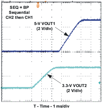 Figure 18. SEQ Pin TIed to BP
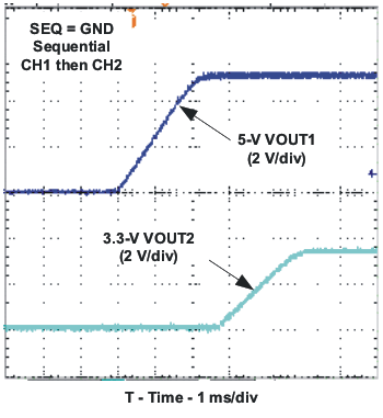 Figure 19. SEQ Pin Tied to GND
NOTE
An R-C network connected to the ENx pin may be used in addition to the SEQ pin in sequential mode to delay the startup of the first output voltage. This approach may be necessary in systems with a large number of output voltages and elaborate voltage sequencing requirements. SeeEnable and Timed Turn On of the Outputs.
If the SEQ pin is left floating, Output 1 and Output 2 each start ratiometrically when both outputs are enabled at the same time. Output 1 and Output 2 soft-start at a rate that is determined by the respective final output voltages and enter regulation at the same time. If the EN1 and EN2 pins are allowed to operate independently, then the two outputs also operate independently.
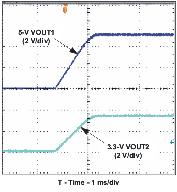 Figure 20. SEQ Pin Floating
7.3.6 Soft-Start
Each output has a dedicated soft-start circuit. The soft-start voltage is an internal digital reference ramp to one of two noninverting inputs of the error amplifier. The other input is the (internal) precision 0.8-V reference. The total ramp time for the FB voltage to charge from 0 V to 0.8 V is about 2.1 ms. During a soft-start interval, the TPS5438x output slowly increases the voltage to the noninverting input of the error amplifier. In this way, the output voltage ramps up slowly until the voltage on the noninverting input to the error amplifier reaches the internal 0.8 V reference voltage. At that time, the voltage at the noninverting input to the error amplifier remains at the reference voltage.
NOTE
To avoid a disturbance in the output voltage during the stepping of the digital soft -tart, a minimum output capacitance of 50μF is recommended. See Feedback Loop and Inductor-Capacitor (L-C) Filter Selection Once the filter and compensation components have been established, laboratory measurements of the physical design should be performed to confirm converter stability.
During the soft-start interval, pulse-by-pulse current limiting is in effect. If an overcurrent pulse is detected, six PWM pulses are skipped to allow the inductor current to decay before another PWM pulse is applied. (See the Output Overload Protection section.) There is no pulse skipping if a current limit pulse is not detected.
DESIGN HINT
If the rate of rise of the input voltage (PVDDx) is such that the input voltage is too low to support the desired regulation voltage by the time Soft-Start has completed, then the output UV circuit may trip and cause a hiccup in the output voltage. In this case, use a timed delay startup from the ENx pin to delay the startup of the output until the PVDDx voltage has the capability of supporting the desired regulation voltage. See Operating Near Maximum Duty Cycleand Maximum Output Capacitance for related information.
7.3.7 Output Voltage Regulation
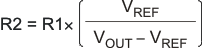
Each output has a dedicated feedback loop comprised of a voltage setting divider, an error amplifier, a pulse width modulator, and a switching MOSFET. The regulation output voltage is determined by a resistor divider connecting the output node, the FBx pin, and GND (see Figure 21). Assuming the value of the upper voltage setting divider is known, the value of the lower divider resistor for a desired output voltage is calculated by Equation 2.
where
- VREF is the internal 0.8-V reference voltage
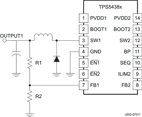 Figure 21. Feedback Network for Channel 1
DESIGN HINT
There is a leakage current of up to 12 μA out of the SW pin when a single output of the TPS5438x is disabled. Keeping the series impedance of R1 + R2 less than 50 kΩ prevents the output from floating above the reference voltage while the controller output is in the OFF state.
7.3.8 Feedback Loop and Inductor-Capacitor (L-C) Filter Selection
In the feedback signal path, the output voltage setting divider is followed by an internal gM-type error amplifier with a typical transconductance of 30 μS. An internal series connected R-C circuit from the gM amplifier output to ground serves as the compensation network for the converter. The signal from the error amplifier output is then buffered and combined with a slope compensation signal before it is mirrored to be referenced to the SW node. Here, it is compared with the current feedback signal to create a pulse-width-modulated (PWM) signal-fed to drive the upper MOSFET switch. A simplified equivalent circuit of the signal control path is depicted in Figure 22.
NOTE
Noise coupling from the SWx node to internal circuitry of BOOTx may impact narrow pulse width operation, especially at load currents less than 1 A. See SW Node Ringing for further information on reducing noise on the SWx node.
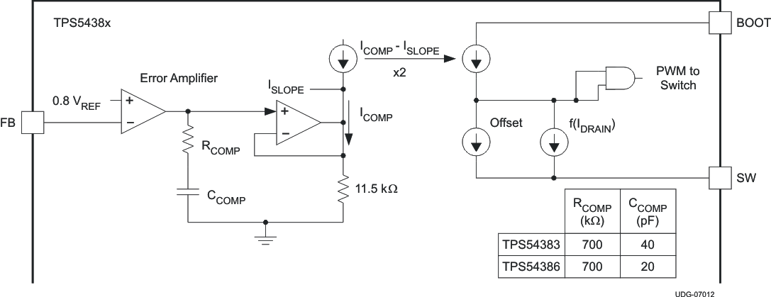 Figure 22. Feedback Loop Equivalent Circuit
A more conventional small signal equivalent block diagram is shown in Figure 23. Here, the full closed loop signal path is shown. Because the TPS5438x contains internal slope compensation and loop compensation components, the external L-C filter must be selected appropriately so that the resulting control loop meets criteria for stability. This approach differs from an externally-compensated controller, where the L-C filter is generally selected first, and the compensation network is found afterwards. To find the appropriate L and C filter combination, the Output-to-Vc signal path plots (see the next section) of gain and phase are used along with other design criterial to aid in finding the combinations that best results in a stable feedback loop.
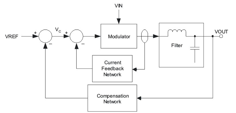 Figure 23. Small Signal Equivalent Block Diagram
7.3.9 Inductor-Capacitor (L-C) Selection
The following figures plot the TPS5438x Output-to-Vc gain and phase versus frequency for various duty cycles (10%, 30%, 50%, 70%, 90%) at three (200 mA, 400 mA, 600 mA) peak-to-peak ripple current levels. The loop response curve selected to compensate the loop is based on the duty cycle of the application and the ripple current in the inductor. Once the curve has been selected and the inductor value has been calculated, the output capacitor is found by calculating the L-C resonant frequency required to compensate the feedback loop. A brief example follows the curves.
Note that the internal error amplifier compensation is optimized for output capacitors with an ESR zero frequency between 20 kHz and 60 kHz. See the following sections for further details.
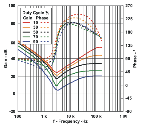 Figure 24. Gain and Phase vs Frequency. TPS54383 at 200-mApp Ripple Current
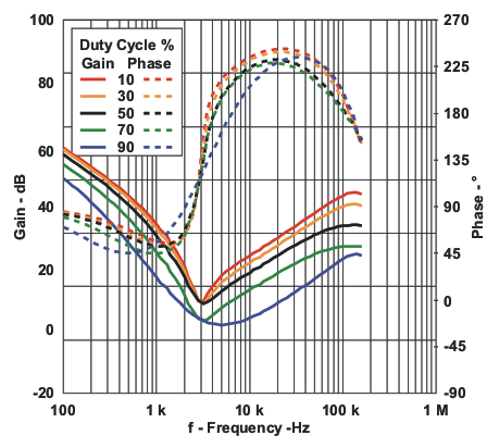 Figure 26. Gain and Phase vs Frequency. TPS54383 at 600-mApp Ripple Current
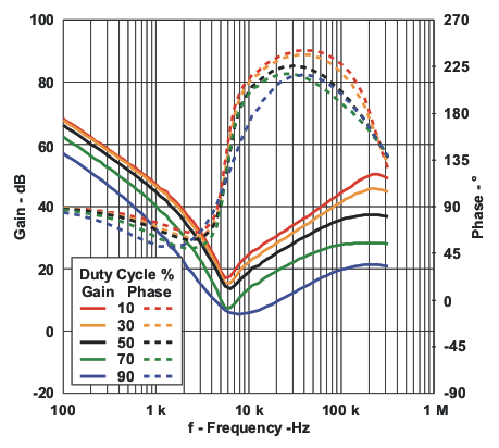 Figure 28. Gain and Phase vs Frequency. TPS54386 at 400-mApp Ripple Current
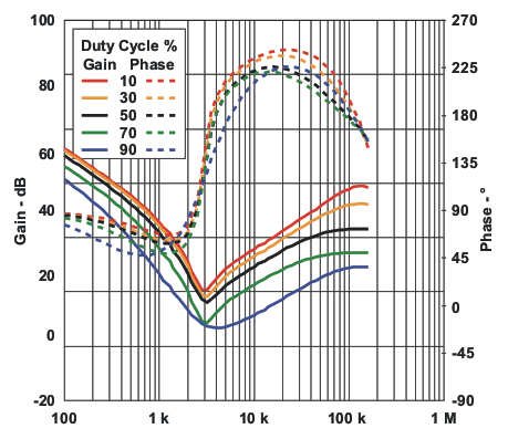 Figure 25. Gain and Phase vs Frequency. TPS54383 at 400-mApp Ripple Current
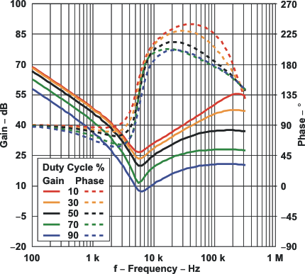 Figure 27. Gain and Phase vs Frequency. TPS54386 at 200-mApp Ripple Current
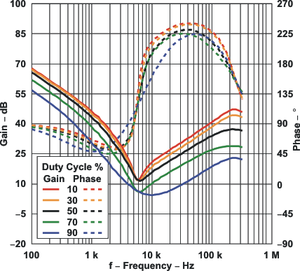 Figure 29. Gain and Phase vs Frequency. TPS54386 at 600-mApp Ripple Current
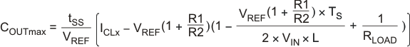
7.3.10 Maximum Output Capacitance
With internal pulse-by-pulse current limiting and a fixed soft-start time, there is a maximum output capacitance which may be used before startup problems begin to occur. If the output capacitance is large enough so that the device enters a current limit protection mode during startup, then there is a possibility that the output will never reach regulation. Instead, the TPS5438x simply shuts down and attempts a restart as if the output were short-circuited to ground. The maximum output capacitance (including bypass capacitance distributed at the load) is given by Equation 3:
7.3.11 Minimum Output Capacitance
Ensure the value of capacitance selected for closed loop stability is compatible with the requirements of Soft-Start.
7.3.12 Modifying The Feedback Loop
Within the limits of the internal compensation, there is flexibility in the selection of the inductor and output capacitor values. A smaller inductor increases ripple current, and raises the resonant frequency, thereby incerasing the required amount of output capacitance. A smaller capacitor could also be used, increasing the resonant frequency, and increasing the overall loop bandwidth—perhaps at the expense of adequate phase margin.
The internal compensation of the TPS54x8x is designed for capacitors with an ESR zero frequency between 20kHz and 60kHz. It is possible, with additional feedback compensation components, to use capacitors with higher or lower ESR zero frequencies. For either case, the components C1 and R3 (ref.Figure 30 ) are added to re-compensate the feedback loop for stability. In this configuration a low frequency pole is followed by a higher frequency zero. The placement of this pole-zero pair is dependent on the type of output capacitor used, and the desired closed loop frequency response.
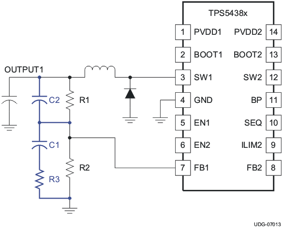 Figure 30. Optional Loop Compensation Components
NOTE
Once the filter and compensation components have been established, laboratory measurements of the physical design should be performed to confirm converter stability.
7.3.12.1 Using High-ESR Output Capacitors
If a high-ESR capacitor is used in the output filter, a zero appears in the loop response that could lead to instability. To compensate, a small R-C series connected network is placed in parallel with the lower voltage setting divider resistor (see Figure 30). The values of the components are determined such that a pole is placed at the same frequency as the ESR zero and a new zero is placed at a frequency location conducive to good loop stability.
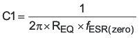
The value of the resistor is calculated using a ratio of impedances to match the ratio of ESR zero frequency to the desired zero frequency.
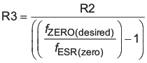
where
- fESR(zero) is the ESR zero frequency of the output capacitor.
- fZERO(desired) is the desired frequency of the zero added to the feedback. This frequency should be placed between 20 kHz and 60 kHz to ensure good loop stability.
The value of the capacitor is calculated in Equation 5.
where
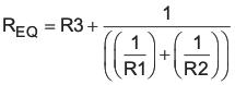
- REQ is an equivalent impedance created by the parallel combination of the voltage setting divider resistors (R1 and R2) in series with R3.
7.3.12.2 Using All Ceramic Output Capacitors
With low ESR ceramic capacitors, there may not be enough phase margin at the crossover frequency. In this case, (see Figure 30) resistor R3 is set equal to 1/2 R2. This lowers the gain by 6 dB, reduce the crossover frequency, and improve phase margin.
The value of C1 is found by determining the frequency to place the low frequency pole. The minimum frequency to place the pole is 1 kHz. Any lower, and the time constant will be too slow and interfere with the internal soft-start (see Soft-Start). The upper bound for the pole frequency is determined by the operating frequency of the converter. It is 3 kHz for the TPS54x83, and 6 kHz for the TPS54x86. C1 is then found from Equation 7. Keep component tolerances in mind when selecting the desired pole frequency.
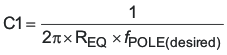
where
- fPOLE(desired)is the desired pole frequency between 1 kHz and 3 kHz (TPS54x83) or 1 kHz and 6 kHz (TPS54x86).
- REQ is an equivalent impedance created by the parallel combination of the voltage setting divider resistors (R1 and R2) in series with R3.
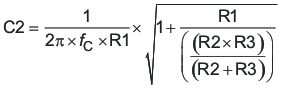
If it is necessary to increase phase margin, place a capacitor in parallel with the upper voltage setting divider resistor (Ref. C2 in Equation 9).
where
- fC is the unity gain crossover frequency, (approximately 50 kHz for most designs following these guidelines)
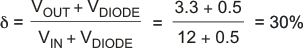
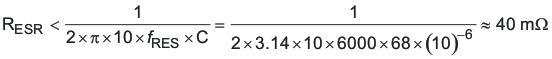
7.3.13 Example: TPS54386 Buck Converter Operating at 12-V Input, 3.3-V Output and 400-mA(P-P) Ripple Current
First, the steady state duty cycle is calculated. Assuming the rectifier diode has a voltage drop of 0.5 V, the duty cycle is approximated using Equation 10.
The filter inductor is then calculated; see Equation 11.
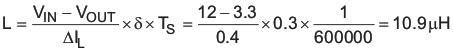
A custom-designed inductor may be used for the application, or a standard value close to the calculated value may be used. For this example, a standard 10-μH inductor is used. Using Figure 28, find the 30% duty cycle curve. The 30% duty cycle curve has a down slope from low frequency and rises at approximately 6 kHz. This curve is the resonant frequency that must be compensated. Any frequency wthin an octave of the peak may be used in calculating the capacitor value. In this example, 6 kHz is used.
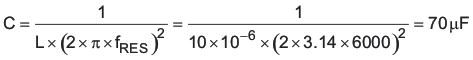
A 68-μF capacitor should be used as a bulk capacitor, with up to 10 μF of ceramic bypass capacitance. To ensure the ESR zero does not significantly impact the loop response, the ESR of the bulk capacitor should be placed a decade above the resonant frequency.
The resulting loop gain and phase are shown in Figure 31. Based on measurement, loop crossover is 45 kHz with a phase margin of 60 degrees.
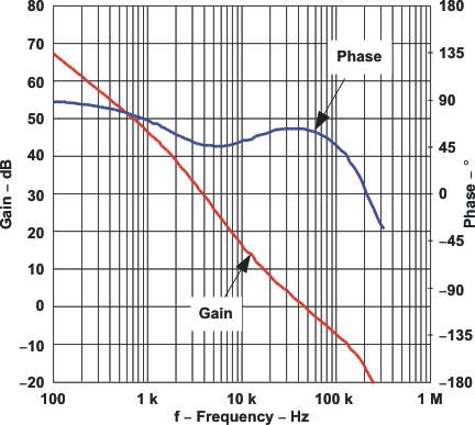 Figure 31. Gain and Phase vs Frequency. Example Loop Result
7.3.14 Bootstrap for the N-Channel MOSFET
A bootstrap circuit provides a voltage source higher than the input voltage and of sufficient energy to fully enhance the switching MOSFET each switching cycle. The PWM duty cycle is limited to a maximum of 90%, allowing an external bootstrap capacitor to charge through an internal synchronous switch (between BP and BOOTx) during every cycle. When the PWM switch is commanded to turn ON, the energy used to drive the MOSFET gate is derived from the voltage on this capacitor.
To allow the bootstrap capacitor to charge each switching cycle, an internal pulldown MOSFET (from SW to GND) is turned ON for approximately 140 ns at the beginning of each switching cycle. In this way, if, during light load operation, there is insufficient energy for the SW node to drive to ground naturally, this MOSFET forces the SW node toward ground and allow the bootstrap capacitor to charge.
Because this is a charge transfer circuit, care must be taken in selecting the value of the bootstrap capacitor. It must be sized such that the energy stored in the capacitor on a per cycle basis is greater than the gate charge requirement of the MOSFET being used.
DESIGN HINT
For the bootstrap capacitor, use a ceramic capacitor with a value between 22 nF and 82 nF.
NOTE
For 5-V input applications, connect PVDDx to BP directly. This connection bypasses the internal control circuit regulator and provides maximum voltage to the gate drive circuitry. In this configuration, shutdown mode IDDSDN will be the same as quiescent IDDQ.
7.3.15 Light Load Operation
There is no special circuitry for pulse skipping at light loads. The normal characteristic of a nonsynchronous converter is to operate in the discontinuous conduction mode (DCM) at an average load current less than one-half of the inductor peak-to-peak ripple current. Note that the amplitude of the ripple current is a function of input voltage, output voltage, inductor value, and operating frequency, as shown in Equation 14.
Further, during discontinuous mode operation the commanded pulse width may become narrower than the capability of the converter to resolve. To maintain the output voltage within regulation, skipping switching pulses at light load conditions is a natural by-product of that mode. This condition may occur if the output capacitor is charged to a value greater than the output regulation voltage, and there is insufficient load to discharge the capacitor. A by-product of pulse skipping is an increase in the peak-to-peak output ripple voltage.
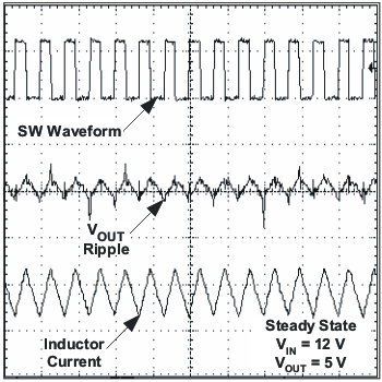 Figure 32. Steady State
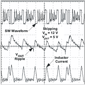 Figure 33. Skipping
DESIGN HINT
If additional output capacitance is required to reduce the output voltage ripple during DCM operation, be sure to recheck Feedback Loop and Inductor-Capacitor (L-C) Filter Selection and Maximum Output Capacitance sections.
7.3.16 SW Node Ringing
A portion of the control circuitry is referenced to the SW node. To ensure jitter-free operation, it is necessary to decrease the voltage waveform ringing at the SW node to less than 5 volts peak and of a duration of less than 30-ns. In addition to following good printed circuit board (PCB) layout practices, there are a couple of design techniques for reducing ringing and noise.
7.3.16.1 SW Node Snubber
Voltage ringing observable at the SW node is caused by fast switching edges and parasitic inductance and capacitance. If the ringing results in excessive voltage on the SW node, or erratic operation of the converter, an R-C snubber may be used to dampen the ringing and ensure proper operation over the full load range.
DESIGN HINT
A series-connected R-C snubber (C = between 330 pF and 1 nF, R = 10 Ω) connected from SW to GND reduces the ringing on the SW node.
7.3.16.2 Bootstrap Resistor
A small resistor in series with the bootstrap capacitor reduces the turn-on time of the internal MOSFET, thereby reducing the rising edge ringing of the SW node.
DESIGN HINT
A resistor with a value between 1Ω and 3Ω may be placed in series with the bootstrap capacitor to reduce ringing on the SW node.
DESIGN HINT
Placeholders for these components should be placed on the initial prototype PCBs in case they are needed.
7.3.17 Output Overload Protection
In the event of an overcurrent during soft-start on either output (such as starting into an output short), pulse-by-pulse current limiting and PWM frequency division are in effect for that output until the internal soft-start timer ends. At the end of the soft-start time, a UV condition is declared and a fault is declared. During this fault condition, both PWM outputs are disabled and the small pulldown MOSFETs (from SWx to GND) are turned ON. This process ensures that both outputs discharge to GND in the event that overcurrent is on one output while the other is not loaded. The converter then enters a hiccup mode timeout before attempting to restart. "Frequency Division" means if an overcurrent pulse is detected, six clock cycles are skipped before a next PWM pulse is initiated, effectively dividing the operating frequency by six and preventing excessive current build up in the inductor.
In the event of an overcurrent on either output after the output reaches regulation, pulse-by-pulse current limit is in effect for that output. In addition, an output undervoltage (UV) comparator monitors the FBx voltage (that follows the output voltage) to declare a fault if the output drops below 85% of regulation. During this fault condition, both PWM outputs are disabled and the small pulldown MOSFETs (from SWx to GND) are turned ON. This design ensures that both outputs discharge to GND, in the event that overcurrent is on one output while the other is not loaded. The converter then enters a hiccup mode timeout before attempting to restart.
The overcurrent threshold for Output 1 is set nominally at 4.5 A. The overcurrent level of Output 2 is determined by the state of the ILIM2 pin. The ILIM setting of Output 2 is not latched in place and may be changed during operation of the converter.
Table 2. Current Limit Threshold Adjustment for Output 2
| ILIM2 Connection | OCP Threshold for Output 2 |
|---|---|
| BP | 4.5 A nominal setting |
| (floating) | 3.0 A nominal setting |
| GND | 1.5 A nominal setting |
DESIGN HINT
The OCP threshold refers to the peak current in the internal switch. Be sure to add one-half of the peak inductor ripple current to the dc load current in determining how close the actual operating point is to the OCP threshold
7.3.18 Operating Near Maximum Duty Cycle
If the TPS5438x operates at maximum duty cycle, and if the input voltage is insufficient to support the output voltage (at full load or during a load current transient), then there is a possibility that the output voltage will fall from regulation and trip the output UV comparator. If this should occur, the TPS5438x protection circuitry will declare a fault and enter a shut down-and-restart cycle.
DESIGN HINT
Ensure that under ALL conditions of line and load regulation, there is sufficient duty cycle to maintain output voltage regulation.
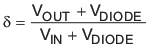
To calculate the operating duty cycle, use Equation 15.
where
- VDIODE is the voltage drop of the rectifier diode
7.3.19 Dual Supply Operation
It is possible to operate a TPS5438x from two supply voltages. If this application is desired, then the sequencing of the supplies must be such that PVDD2 is above the UVLO voltage before PVDD1 begins to rise. This level requirement ensures that the internal regulator and the control circuitry are in operation before PVDD1 supplies energy to the output. In addition, Output 1 must be held in the disabled state (EN1 high) until there is sufficient voltage on PVDD1 to support Output 1 in regulation. (See the Operating Near Maximum Duty Cycle section.)
The preferred sequence of events is:
- PVDD2 rises above the input UVLO voltage
- PVDD1 rises with Output 1 disabled until PVDD1 rises above level to support Output 1 regulation.
With these two conditions satisfied, there is no restriction on PVDD2 to be greater than, or less than PVDD1.
DESIGN HINT
An R-C delay on EN1 may be used to delay the startup of Output1 for a long enough period of time to ensure that PVDD1 can support Output 1 load.
7.3.20 Cascading Supply Operation
It is possible to source PVDD1 from Output 2 as depicted in Figure 34 and Figure 35. This configuration may be preferred if the input voltage is high, relative to the voltage on Output 1.
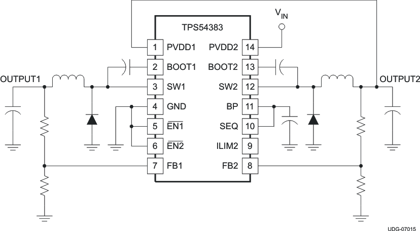 Figure 34. Schematic Showing Cascading PVDD1 from Output 2
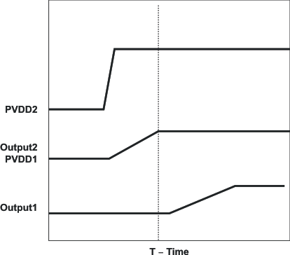 Figure 35. Waveforms Resulting from Cascading PVDD1 from Output 2
In this configuration, the following conditions must be maintained:
- Output 2 must be of a voltage high enough to maintain regulation of Output 1 under all load conditions.
- The sum of the current drawn by Output 2 load plus the current into PVDD1 must be less than the overload protection current level of Output 2.
- The method of output sequencing must be such that the voltage on Output 2 is sufficient to support Output 1 before Output 1 is enabled. This requrement may be accomplished by:
- a delay of the enable function
- selecting sequential sequencing of Output 1 starting after Output 2 is in regulation
7.3.21 Multiphase Operation
The TPS5438x is not designed to operate as a two-channel multiphase converter. See http://www.power.ti.com for appropriate device selection.
7.3.22 Bypass and FIltering
As with any integrated circuit, supply bypassing is important for jitter-free operation. To improve the noise immunity of the converter, ceramic bypass capacitors must be placed as close to the package as possible.
- PVDD1 to GND: Use a 10-μF ceramic capacitor
- PVDD2 to GND: Use a 10-μF ceramic capacitor
- BP to GND: Use a 4.7-μF to 10-μF ceramic capacitor
7.3.23 Overtemperature Protection and Junction Temperature Rise
The overtemperature thermal protection limits the maximum power to be dissipated at a given operating ambient temperature. In other words, at a given device power dissipation, the maximum ambient operating temperature is limited by the maximum allowable junction operating temperature. The device junction temperature is a function of power dissipation, and the thermal impedance from the junction to the ambient. If the internal die temperature should reach the thermal shutdown level, the TPS5438x shuts off both PWMs and remains in this state until the die temperature drops below the hysteresis value, at which time the device restarts.
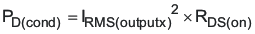
The first step to determine the device junction temperature is to calculate the power dissipation. The power dissipation is dominated by the two switching MOSFETs and the BP internal regulator. The power dissipated by each MOSFET is composed of conduction losses and output (switching) losses incurred while driving the external rectifier diode. To find the conduction loss, first find the RMS current through the upper switch MOSFET.
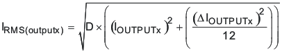
where
- D is the duty cycle
- IOUTPUTx is the dc output current
- ΔIOUTPUTx is the peak ripple current in the inductor for Outputx
Notice the impact of the operating duty cycle on the result.
Multiplying the result by the RDS(on) of the MOSFET gives the conduction loss.
The switching loss is approximated by:
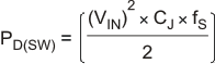
where
- where CJ is the prallel capacitance of the rectifier diode and snubber (if any)
- fS is the switching frequency
The total power dissipation is found by summing the power loss for both MOSFETs plus the loss in the internal regulator.

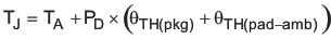
The temperature rise of the device junction depends on the thermal impedance from junction to the mounting pad (See the Thermal Information table for performance on the standard test board), plus the thermal impedance from the thermal pad to ambient. The thermal impedance from the thermal pad to ambient depends on the PCB layout (PowerPAD interface to the PCB, the exposed pad area) and airflow (if any). See the Layout Guidelines section.
The operating junction temperature is shown in Equation 20.
7.3.24 Power Derating
The TPS5438x delivers full current at ambient temperatures up to +85°C if the thermal impedance from the thermal pad maintains the junction temperature below the thermal shutdown level. At higher ambient temperatures, the device power dissipation must be reduced to maintain the junction temperature at or below the thermal shutdown level. Figure 36 illustrates the power derating for elevated ambient temperature under various airflow conditions. Note that these curves assume that the PowerPAD is properly soldered to the recommended thermal pad. (See the Related Documentation section for further information.)
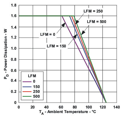 Figure 36. Power Dissipation vs Ambient Temperature. Power Derating Curves
7.4 Device Functional Modes
7.4.1 Minimum Input Voltage
The TPS5438x is recommended to operate with input voltages above 4.5 V. The typical UVLO threshold is 4.1 V at PVDD2 and the device may operate at PVDD2 voltages down to the UVLO voltage. PVDD2 is used for input voltage UVLO protection because it is the power supply for the BP regulator. The device will operate with PVDD1 voltages even lower as long as PVDD2 is above its UVLO threshold. With VPVDD2 below the UVLO voltage threshold the device will not switch. If either ENx pins is pulled below 0.9 V, when VPVDD2 passes the UVLO threshold the BP regulator turns on and begins charging the BP capacitor. After VBP is greater than 4 V, depending on the state of the SEQ pin, the channel corresponding to the low ENx pin will become active. When a channel becomes active switching is enabled and the soft-start sequence is initiated. The TPS5438x starts linearly ramping up an internal soft-start reference voltage of the active channel from 0 V to its final value over the internal soft-start time period. The designer should make sure the input voltage is sufficient to support the output voltage of the active channels.
7.4.2 ENx Control
The enable start threshold voltage is 1.2 V typical. With ENx held above the 1.2 V threshold voltage the correspondeng cahnnel of the TPS548x is disabled and switching is inhibited even if PVDD2 is above its UVLO threshold. The quiescent current is reduced in this state. When the first ENx pin voltage is decreased below the threshold while V(PVDD2) is above the UVLO threshold the BP regulator turns on and begins charging the BP capacitor. After VBP is greater than 4 V, depending on the state of the SEQ pin, the channel corresponding to the low ENx pin will become active. If the second ENx pin voltage is decreased below the threshold after VBP is greater than 4 V, again depending on the state of the SEQ pin, the corresponding channel will become active immediately. When a channel becomes active switching is enabled and the slow-start sequence is initiated. The TPS548x starts linearly ramping up the internal soft-start reference voltage of the active channel from 0 V to its final value over the internal slow-start time period. If both channels are active the start-up sequence is deteremined by the stat of the SEQ pin. The designer should make sure the input voltage is sufficient to support the output voltageof the active channels.