SLUS774C AUGUST 2007 – December 2014
PRODUCTION DATA.
- 1 Features
- 2 Applications
- 3 Description
- 4 Revision History
- 5 Pin Configuration and Functions
- 6 Specifications
-
7 Detailed Description
- 7.1 Overview
- 7.2 Functional Block Diagram
- 7.3
Feature Description
- 7.3.1 Voltage Reference
- 7.3.2 Oscillator
- 7.3.3 Input Undervoltage Lockout (UVLO) and Startup
- 7.3.4 Enable and Timed Turn On of the Outputs
- 7.3.5 Output Voltage Sequencing
- 7.3.6 Soft-Start
- 7.3.7 Output Voltage Regulation
- 7.3.8 Feedback Loop and Inductor-Capacitor (L-C) Filter Selection
- 7.3.9 Inductor-Capacitor (L-C) Selection
- 7.3.10 Maximum Output Capacitance
- 7.3.11 Minimum Output Capacitance
- 7.3.12 Modifying The Feedback Loop
- 7.3.13 Example: TPS54386 Buck Converter Operating at 12-V Input, 3.3-V Output and 400-mA(P-P) Ripple Current
- 7.3.14 Bootstrap for the N-Channel MOSFET
- 7.3.15 Light Load Operation
- 7.3.16 SW Node Ringing
- 7.3.17 Output Overload Protection
- 7.3.18 Operating Near Maximum Duty Cycle
- 7.3.19 Dual Supply Operation
- 7.3.20 Cascading Supply Operation
- 7.3.21 Multiphase Operation
- 7.3.22 Bypass and FIltering
- 7.3.23 Overtemperature Protection and Junction Temperature Rise
- 7.3.24 Power Derating
- 7.4 Device Functional Modes
-
8 Applications and Implementation
- 8.1 Application Information
- 8.2
Typical Applications
- 8.2.1
12-V to 5-V and 3.3-V Converter
- 8.2.1.1 Design Requirements
- 8.2.1.2
Detailed Design Procedure
- 8.2.1.2.1 Duty Cycle Estimation
- 8.2.1.2.2 Inductor Selection
- 8.2.1.2.3 Rectifier Diode Selection
- 8.2.1.2.4 Output Capacitor Selection
- 8.2.1.2.5 Voltage Setting
- 8.2.1.2.6 Compensation Capacitors
- 8.2.1.2.7 Input Capacitor Selection
- 8.2.1.2.8 Boot Strap Capacitor
- 8.2.1.2.9 ILIM
- 8.2.1.2.10 SEQ
- 8.2.1.2.11 Power Dissipation
- 8.2.1.3 Application Curves
- 8.2.2 24-V to 12-V and 24-V to 5-V
- 8.2.3 5-V to 3.3V and 5-V to 1.2 V
- 8.2.1
12-V to 5-V and 3.3-V Converter
- 9 Power Supply Recommendations
- 10Layout
- 11Device and Documentation Support
- 12Mechanical, Packaging, and Orderable Information
10 Layout
10.1 Layout Guidelines
The layout guidelines presented here are illustrated in the PCB layout examples given in Figure 51 and Figure 52.
- The PowerPAD must be connected to a low current (signal) ground plane having a large copper surface area to dissipate heat. Extend the copper surface well beyond the IC package area to maximize thermal transfer of heat away from the IC.
- Connect the GND pin to the PowerPAD through a 10-mil (.010 in, or 0.0254 mm) wide trace.
- Place the ceramic input capacitors close to PVDD1 and PVDD2; connect using short, wide traces.
- Maintain a tight loop of wide traces from SW1 or SW2 through the switch node, inductor, output capacitor and rectifier diode. Avoid using vias in this loop.
- Use a wide ground connection from the input capacitor to the rectifier diode, placed as close to the power path as possible. Placement directly under the diode and the switch node is recommended.
- Locate the bootstrap capacitor close to the BOOT pin to minimize the gate drive loop.
- Locate voltage setting resistors and any feedback components over the ground plane and away from the switch node and the rectifier diode to input capacitor ground connection.
- Locate snubber components (if used) close to the rectifier diode with minimal loop area.
- Locate the BP bypass capacitor very close to the IC; a minimal loop area is recommended.
- Locate the output ceramic capacitor close to the inductor output terminal between the inductor and any electrolytic capacitors, if used.
10.2 Layout Example
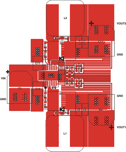 Figure 51. Top Layer Copper Layout and Component Placement
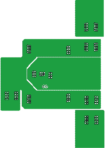 Figure 52. Bottom Layer Copper Layout
10.3 PowerPAD Package
The PowerPAD package provides low thermal impedance for heat removal from the device. The PowerPAD derives its name and low thermal impedance from the large bonding pad on the bottom of the device. The circuit board must have an area of solder-tinned-copper underneath the package. The dimensions of this area depend on the size of the PowerPAD package. Thermal vias connect this area to internal or external copper planes and should have a drill diameter sufficiently small so that the via hole is effectively plugged when the barrel of the via is plated with copper. This plug is needed to prevent wicking the solder away from the interface between the package body and the solder-tinned area under the device during solder reflow. Drill diameters of 0.33 mm (13 mils) work well when 1-oz. copper is plated at the surface of the board while simultaneously plating the barrel of the via. If the thermal vias are not plugged when the copper plating is performed, then a solder mask material should be used to cap the vias with a diameter equal to the via diameter of 0.1 mm minimum. This capping prevents the solder from being wicked through the thermal vias and potentially creating a solder void under the package. (See the Related Documentation section.)