SLUU182A January   2004  – March 2022 TPS5124


  1.   Trademarks
  2. 1Introduction
  3. 2Features
  4. 3Schematic
  5. 4Design Procedure
    1. 4.1 Frequency Setting
    2. 4.2 Inductance Value
    3. 4.3 Output Capacitors
    4. 4.4 Input Capacitors
      1. 4.4.1 Case One: D1, D2 < 0.5
      2. 4.4.2 Case Two: D2 < 0.5 < D1
    5. 4.5 Compensation Design
    6. 4.6 Current Limiting
    7. 4.7 Timer Latch
      1. 4.7.1 Undervoltage Protection
      2. 4.7.2 Short Circuit Protection
      3. 4.7.3 Overvoltage Protection
      4. 4.7.4 Disabling the Protection Function
        1. 4.7.4.1 Disabling the Overcurrent Protection
        2. 4.7.4.2 Disabling the Overvoltage Protection or Undervoltage Protection
  6. 5Test Results
    1. 5.1 Efficiency Curves
    2. 5.2 Typical Operating Waveform
    3. 5.3 Start-Up Waveform
    4. 5.4 Output Ripple Voltage and Load Transient
  7. 6Layout Guidelines
    1. 6.1 Low-Side MOSFET
    2. 6.2 Connections
    3. 6.3 Bypass Capacitor
    4. 6.4 Bootstrap Capacitor
    5. 6.5 Output Voltage
  8. 7PCB Layout
  9. 8List of Materials
  10. 9Revision History

Input Capacitors

Due to the out-of-phase operation, the input current ripple is partially canceled. The total RMS current in the input capacitor is calculated as follows. This assumes the total input current goes into the input capacitor to the power ground and ignores the ripple current in the inductor.
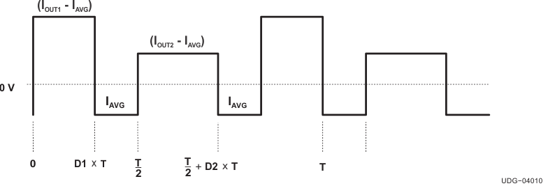
GUID-20220302-SS0I-KNDT-GKRL-RRRQJB1W2B3N-low.gif Figure 4-1 Case One (D1 < 0.5, D2 < 0.5)
GUID-20220302-SS0I-7BXT-14KQ-JQXKL0JZ0BP0-low.gif Figure 4-2 Case Two (D2 < 0.5 < D1)