SLUUCE9A December 2020 – April 2021 TPS543820 , TPS543820E
- Trademarks
- 1Introduction
- 2Configurations and Modifications
-
3Test Setup and Results
- 3.1 Input/Output Connections
- 3.2 Efficiency
- 3.3 Output Voltage Regulation
- 3.4 Load Transient and Loop Response
- 3.5 Output Voltage Ripple
- 3.6 Input Voltage Ripple
- 3.7 Synchronizing to a Clock
- 3.8 Start-up and Shutdown with EN
- 3.9 Start-up and Shutdown with VIN
- 3.10 Start-up Into Pre-Bias
- 3.11 Hiccup Current Limit
- 3.12 Overvoltage Protection
- 3.13 Thermal Performance
- 4Board Layout
- 5Schematic and Bill of Materials
- 6Revision History
3.13 Thermal Performance
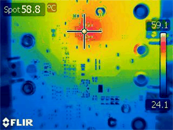
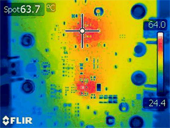
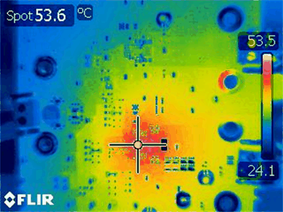
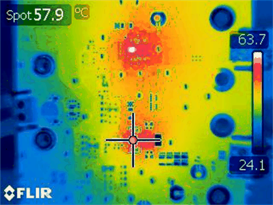
Figure 3-40 through Figure 3-43 show the temperature rise of the TPS543820 ICs at full 8-A load. Figure 3-40 and Figure 3-41 have only one TPS543820 on and loaded. Figure 3-42 and Figure 3-43 have both TPS543820s loaded. A minimum of a 10 minute soak time was used before taking each measurement.
 Figure 3-40 U1
Thermal Performance – 8-A
Load and U2 off
 Figure 3-42 U1
Thermal Performance – Both 8-A Load
 Figure 3-41 U2
Thermal Performance – 8-A
Load and U1 off
 Figure 3-43 U2
Thermal Performance – Both 8-A Load