SLUUCH0 April 2022 LMR51430
3 PCB Layouts
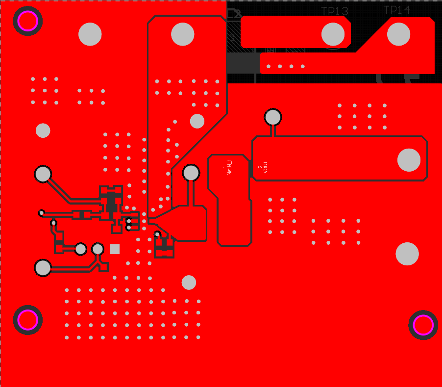
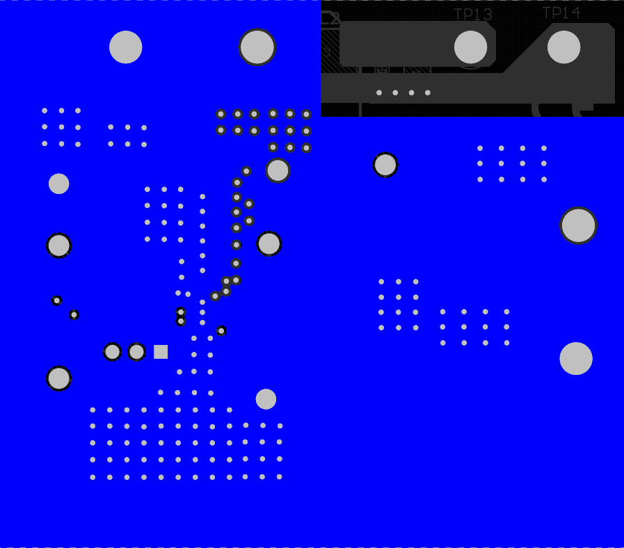
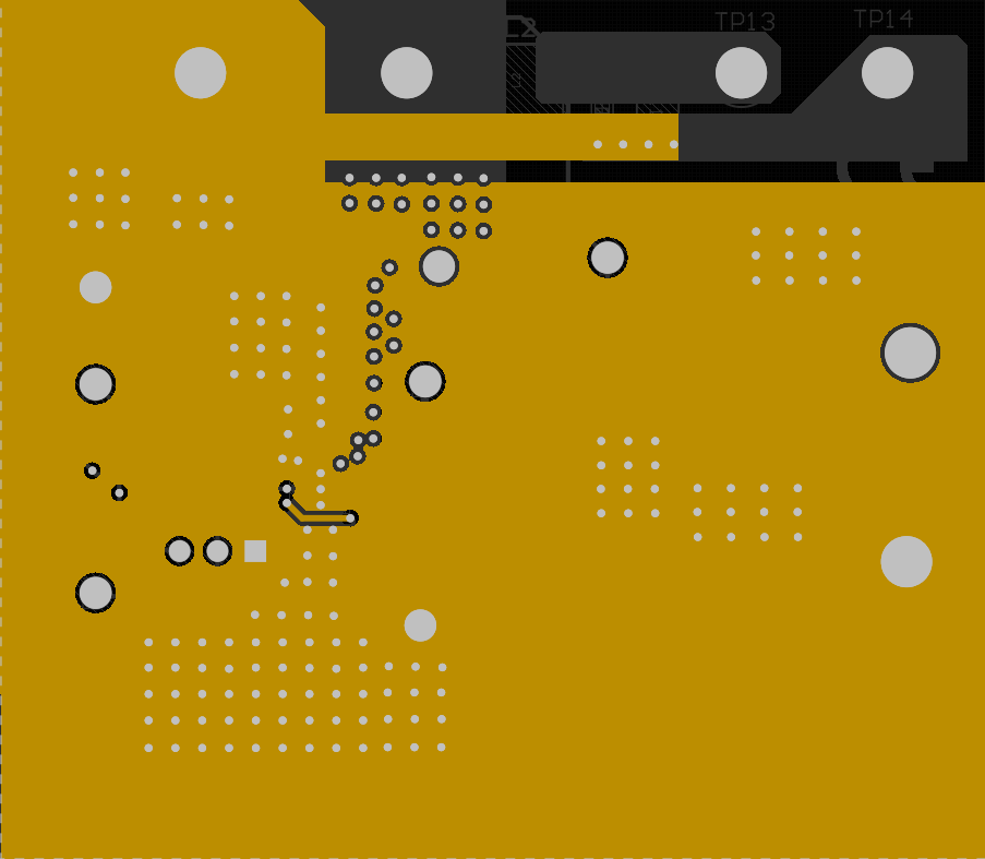
Figure 3-1 to Figure 3-2 show the board layout for the LMR51430EVM. The PCB consists of a 4-layer design. The board size is 57.8-mm × 64mm, 2-oz copper planes are applied on each layers.
 Figure 3-1 PCB Layout (Top View)
 Figure 3-2 PCB Layout (Bottom View)
 Figure 3-3 Layer 1
 Figure 3-4 Layer 2