SLUUCS5A january   2023  – july 2023 UCC14141-Q1


  1.   1
  2.   Abstract
  3.   Trademarks
  4. 1Introduction
    1. 1.1 U1 Component Selection
    2. 1.2 Pin Configuration and Functions
  5. 2Description
    1. 2.1 EVM Electrical Performance Specifications
  6. 3Schematic
  7. 4EVM Setup and Operation
    1. 4.1 Recommended Test Equipment
    2. 4.2 External Connections for Easy Evaluation
    3. 4.3 Powering the EVM
      1. 4.3.1 Power on for Start-up
      2. 4.3.2 Power off for Shutdown
    4. 4.4 EVM Test Points
    5. 4.5 Probing the EVM
  8. 5 Performance Data
    1. 5.1  Efficiency Data
    2. 5.2  Regulation Data
    3. 5.3  Steady State Input Current
    4. 5.4  Start-up Waveforms
    5. 5.5  Inrush Current
    6. 5.6  AC Ripple Voltage
    7. 5.7  EN-to-/PG Timing
    8. 5.8  RLIM
    9. 5.9  Fault Protection
      1. 5.9.1 Output UVLO
      2. 5.9.2 Output OVP
    10. 5.10 Shutdown
    11. 5.11 Thermal Performance
  9. 6Assembly and Printed Circuit Board (PCB) Layers
  10. 7Bill of Materials (BOM)
  11. 8Revision History

Assembly and Printed Circuit Board (PCB) Layers

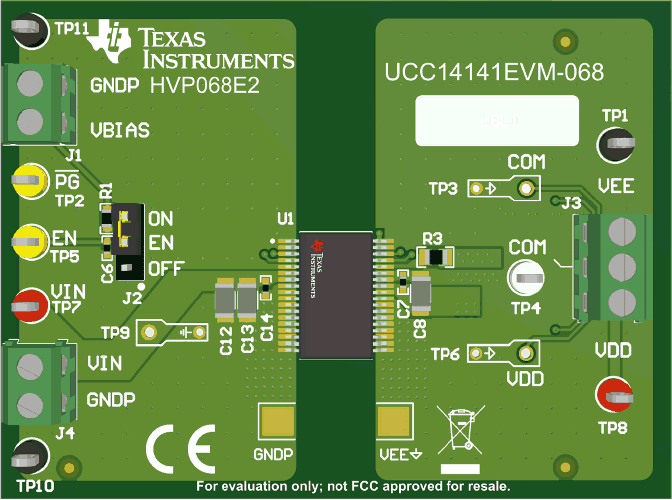
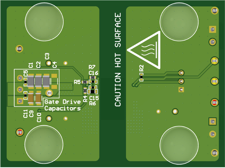
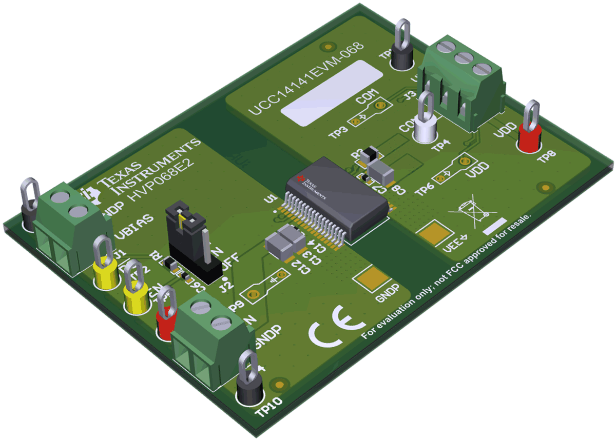
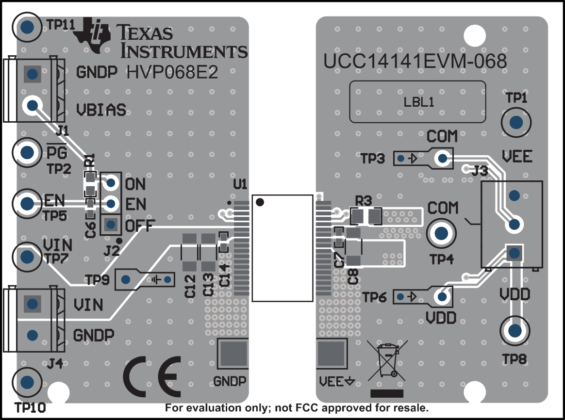
The UCC14141EVM-068 is designed using a four-layer, FR4, PCB, fabricated with 2-ounce copper on all four layers. The EVM, PCB demonstrates the important use of ground planes and tented stitching vias for shielding and improving EMI performance. For higher density PCBs such as automotive traction inverters, the PCB can include several additional signal layers but similar design methodology can be applied as best as possible.

GUID-20230203-SS0I-HLMM-F6B1-VC244RQPDKFG-low.png

Figure 6-1 UCC14141EVM-068, Fully Assembled 3D Top View
GUID-20230203-SS0I-WWWV-RPV6-QVGZ5GL0H3WT-low.png

Figure 6-2 UCC14141EVM-068, Fully Assembled 3D Bottom View
GUID-20230203-SS0I-VWQ1-JBCG-CHRLHMVTXLZQ-low.png

Figure 6-3 UCC14141EVM-068, 3D Angle View
GUID-20230203-SS0I-JZJ7-DNDS-PTHHWDV58TKN-low.gif

Figure 6-4 UCC14141EVM-068, PCB Top Layer, Assembly
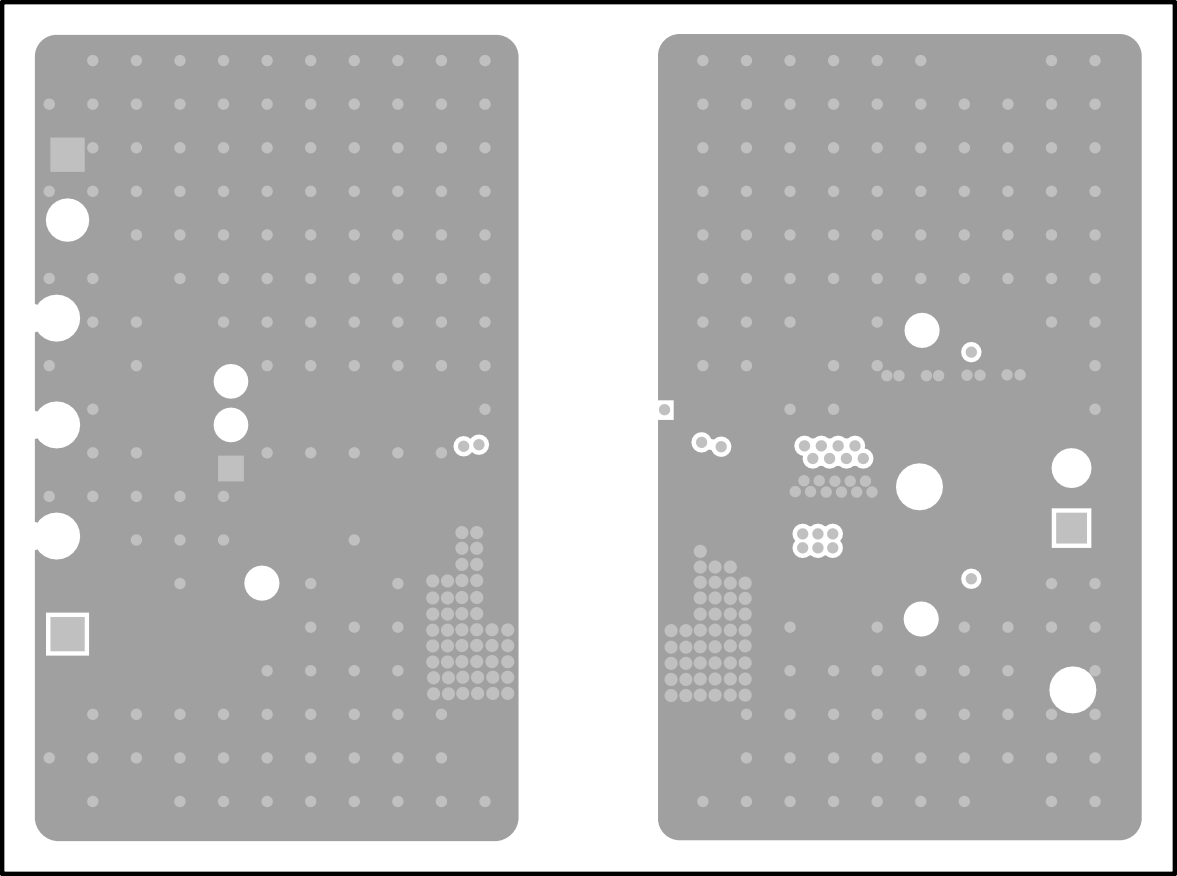
GUID-20230203-SS0I-KZVD-VF2Z-GCXFWS0MSXXQ-low.gif

Figure 6-5 UCC14141EVM-068, GND Layer 2 (same as layer 3)

GUID-20230203-SS0I-KZVD-VF2Z-GCXFWS0MSXXQ-low.gif

Figure 6-6 UCC14141EVM-068, GND Layer 3 (same as layer 2)
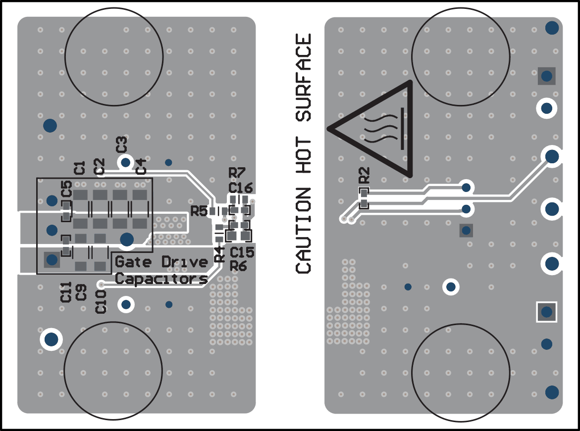
GUID-20230203-SS0I-5TDF-3L8B-F7LPJFFCTZJG-low.gif

Figure 6-7 UCC14141EVM-068, PCB Bottom Layer, Assembly (mirrored view)