SLVA478C October 2013 – November 2022 TPS62120 , TPS62122
4.3 Selecting L and COUT for Stability
The switch node, inductor current, and the output voltage ripple during steady state are signals that need to be checked first for the stability of the system. Oscillations on the output voltage and the inductor current, and jitter on the switch node are good indicators of the instability of the system. Figure 5-7 shows both the switch node and output voltage ripple of this topology. Load transient response is another good test for stability, as described in the SLVA381 application report.
The recommended nominal inductor and output capacitor values to use for this topology are in the range of 18 µH to 22 µH and from 10 µF to 47 µF, respectively. In this application report, a 18-µH inductor and a 10-µF capacitor are used.
The inverting buck boost topology contains a Right Half Plane (RHP) zero which significantly and negatively impacts the control loop response by adding an increase in gain along with a decrease in phase at a high frequency. This can cause instability. Equation 4 estimates the frequency of the RHP zero.
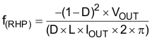
It is recommended to keep the loop crossover frequency to 1/10th of the RHP zero frequency. Doing this requires either decreasing the inductance to increase the RHP zero frequency or increasing the output capacitance to decrease the crossover frequency. Note that the RHP zero frequency occurs at lower frequencies with lower input voltages, which have a higher duty cycle. SLVA465 explains how to measure the control loop of a DCS-Control™ device while Figure 4-2 shows the bode plot of Figure 5-1.
 Figure 4-2 Bode Plot at 5-V VIN and 50-mA Load