SLVA793A june 2016 – august 2023 ESD122 , ESDS304 , TPD1E04U04 , TPD2E1B06 , TPD2EUSB30 , TPD4E004 , TPD4E02B04 , TPD4E05U06-Q1 , TPD6E004
2 Why Impedance Mismatches Matter
Any mismatch in impedance at the node where the ESD protection diode connects to the transmission line has an impact on the signal integrity. The effect from a mismatch in impedance on a voltage-varying signal propagating down a transmission line is to reflect back some voltage towards the source, of which some voltage can then reflect back again if there is another change in impedance. This back and forth reflection continues through the line wherever there are any impedance mismatches. Depending on the distance between the impedance mismatches, the signal may be attenuated or amplified due to any part of the signal that has been reflected back and forth being added to the signal propagating down the line. If the impedance mismatches are big enough, then these reflections can change the voltage levels of the signal outside of the receivers input logic levels, leading to a loss of data.
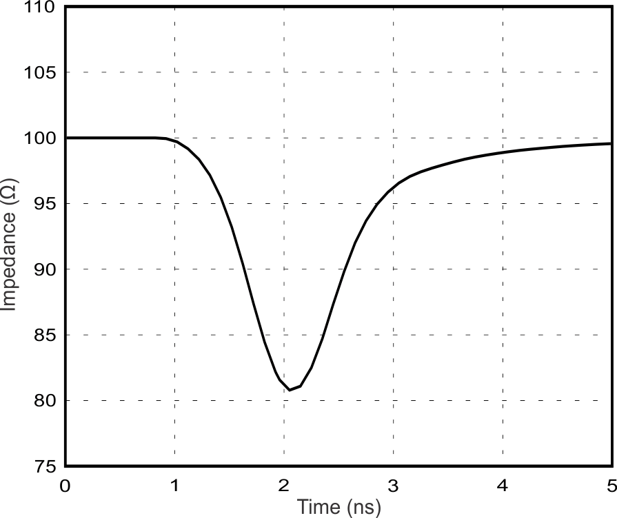
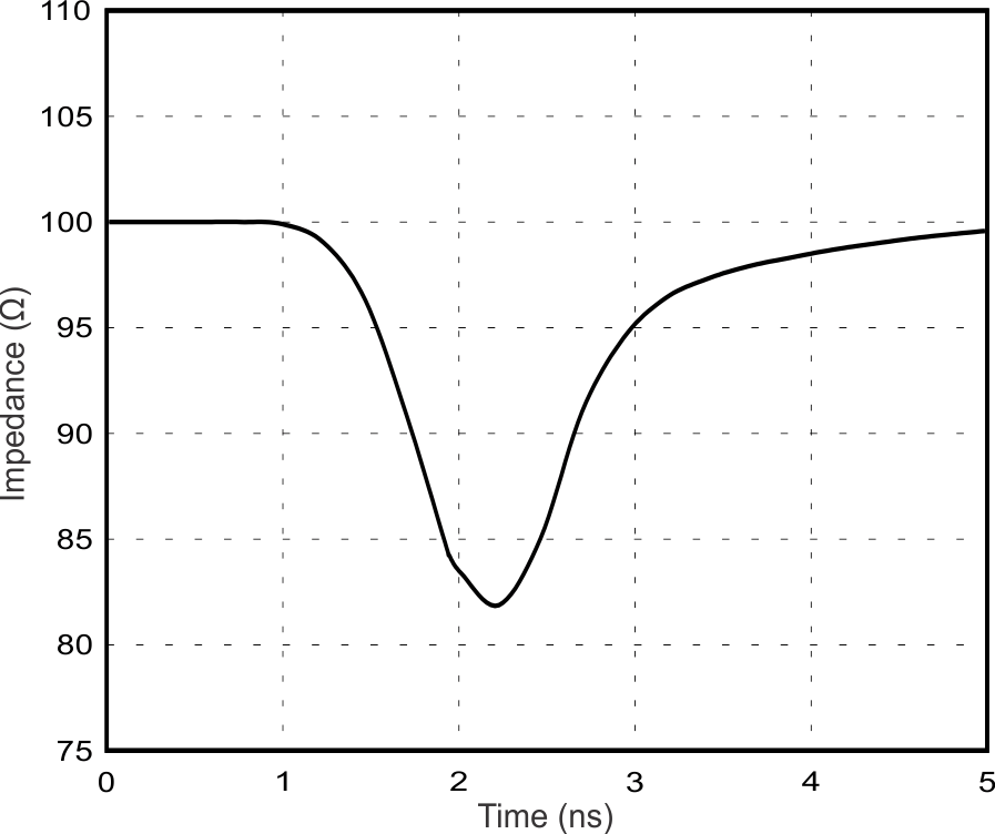
Some industry specifications stipulate how much total parasitic capacitance a source or a sink can have, not including what resides in the receiver chipset. For USB 3.1 Gen 1 this is 1.25 pF for a source and for Gen 2 it is 1.1 pF. Other industry specifications do not specify the capacitance by value, but rather by the impact on the characteristic impedance of the transmission line when measured by a time domain reflectometer (TDR) using a specified rise-time. The HDMI 2.0 specification stipulates no single excursion beyond 100 Ω ±25% for a duration of 250 ps when measured with a TDR rise-time of less 200 ps. Impedance for some Texas Instruments ESD diodes are shown in Figure 2-2 and Figure 2-3.
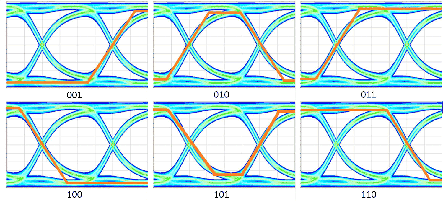
Controlling the impedance in a transmission line is paramount to maintaining good signal integrity. One of the most useful tools for verifying good signal integrity is the data eye diagram. The data eye diagram is comprised of every unit interval in a multi-bit pseudo-random bit sequence (PRBS) signal superimposed on one another. Figure 2-1 show six example transitions mapped by the eye diagram.
 Figure 2-1 Binary Code in an Eye Diagram
 Figure 2-2 Impedance of TPD1E04U04DPY from 192-ps Rise-Time
TDR
 Figure 2-3 Impedance of TPD4E02B04DQA from 192-ps Rise-Time
TDR