SLVAF01 October 2020 TPS55340
2.2 Forward Recovery Characteristic of Blocking Diode
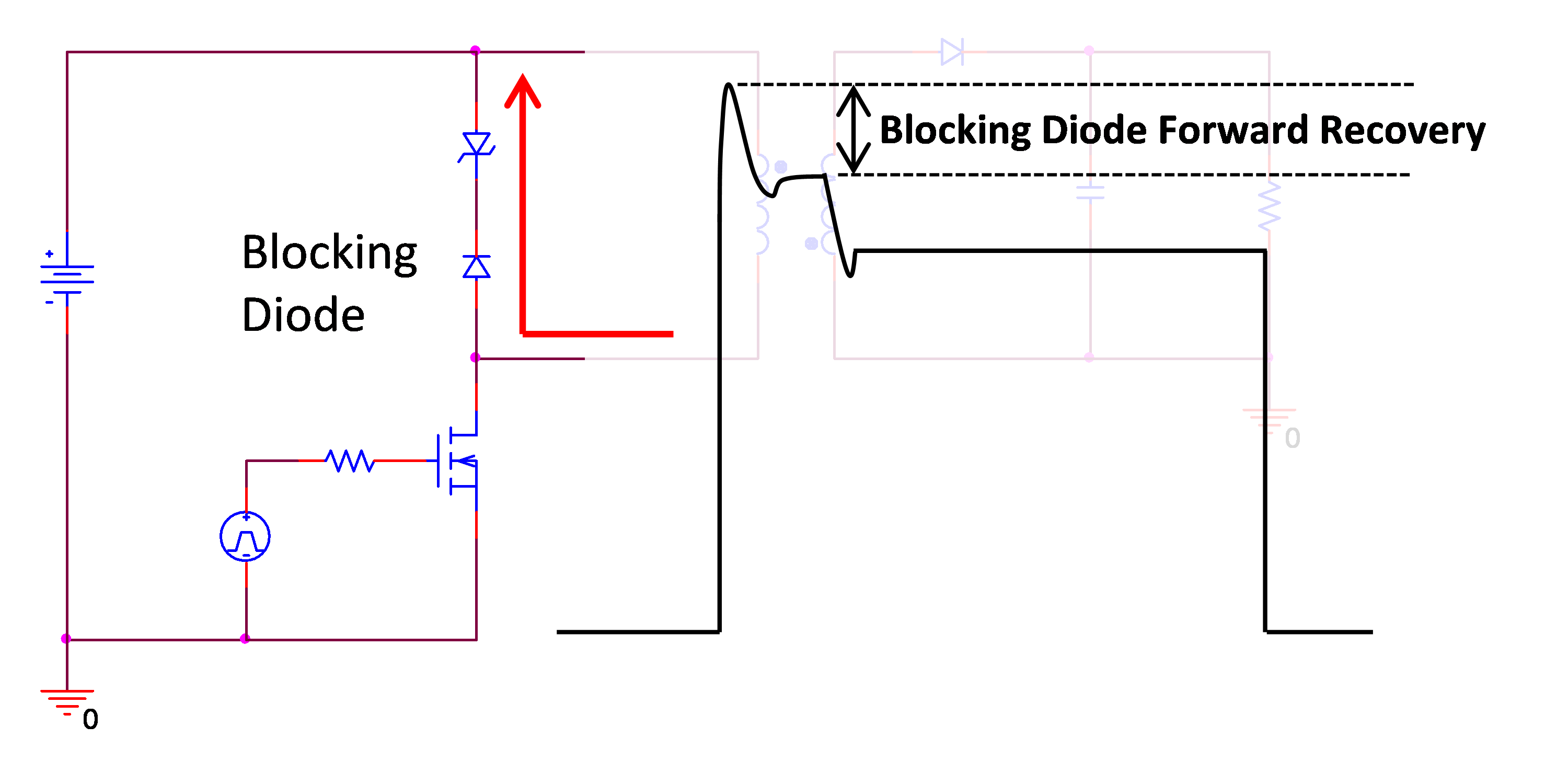
At turn off transient, the stored energy in leakage inductance should be dissipated through zener as fast as possible. Before the turn off stage, the blocking diode is in reverse biased and then it should immediately flow the current from leakage inductance to zener diode when the main switch is turned off. So the path to zener in the layout should be decent, but the forward recovery time of blocking diode is also important factor as well. If the blocking diode’s speed is not enough to handle this transient energy, it will bring up an unwanted voltage peak. Figure 2-3 highlights the portion which is being built during blocking diode’s forward recovery period. In a real test result from Figure 3-1, around 5 V of the voltage peaking is linked to this time.
 Figure 2-3 Voltage Peaking from Forward
Recovery of blocking Diode