SLVAF37 January 2021 ATL431LI
2.3 Schematic Analysis and Waveforms
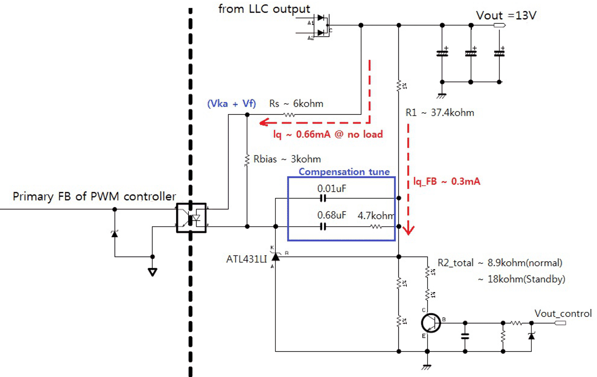
 Figure 2-5 ATL431LI Design Review in LLC
Schematic
Figure 2-5 ATL431LI Design Review in LLC
SchematicFigure 2-5 shows a good starting value and it tells how much total power consumption in the feedback loop is consumed. We see about 1mA from two quiescent current paths. Probably designer would expect <15mW at beginning. However we still have more room to reduce it based on performance advantages of ATL43xLI. The optional Rbias also can contribute effort to minimize loss in tune. In case of system standby mode, which lowers the Vout level, the amount of consumption would decrease more. Let’s define operating behaviors from measured waveforms.
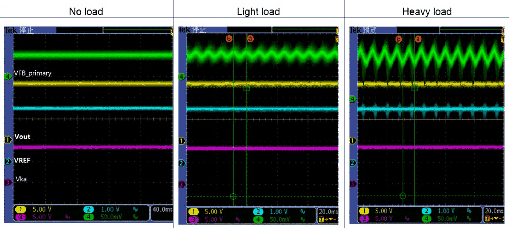
 Figure 2-6 No Load, Light Load, and Heavy
Load
Figure 2-6 No Load, Light Load, and Heavy
LoadTable 2-1 will give designers easy understanding to clarify how the system works. And it would request users to refer to block-diagram of shunt regulator. One note is that reflected VFB_primary are fully dependent on how PWM controller handles it. The Vka is an error amplifier signal decided by feedback loop including compensation network and it also varies in a little change according to optocoupler’s CTR and configuration of primary side.
| Transient | NPN I_base | NPN I_sink | Vka(cathode) | Ika | I_opto | PWM duty | |
|---|---|---|---|---|---|---|---|
| REF > VREF | Increased | Increased | Drop | Increased | Increased | Reduced | till VREF > REF |
| REF < VREF | Decreased | Decreased | Rise | Decreased | Decreased | Expand | till REF > VREF |