SLVAF37 January 2021 ATL431LI
2.2 Design Considerations for Biasing Circuit
We now understand how the feedback loop is configured and can categorize the current flow in the loop. Sufficient bias current would make a system stable but we know there are Standard Energy requirements to meet, such as DoE level VI in US and CoC tier 2 in EU. It means designers should take the limitations from total standby power consumption.
Before started, let’s take one premise again that system accuracy by variation factors are fixed. We can find electrical parameters have error range and it would result in Vout error, current consumption error etc in the system. Regarding how managing those matters, see the Designing with the Improved TL431LI application note. Also, advanced product – ATL43xLI can be biased with lower cathode current (IKA) and provide improved bandwidth compared to TL43x. Regarding the benefits detail, see the Designing with the ATL431LI in Flyback Converters application note.
Step 1: Check out standby Iq consumption from two paths, at a given power consumption budget.
 Figure 2-4 Quiescent Current Paths in the
Feedback
Figure 2-4 Quiescent Current Paths in the
Feedback Step 2: Compute required Rs. The IKA bias current is limited by the value of Rs.
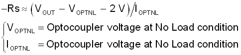
For further explanation, system designer should set a proper IOPTNL first. We design it close to IKA(min) * 1.5 at worst case which includes a margin. And then, we can find required VOPTNL from the data sheet of optocoupler selected. Generally it will be about 1 V. Lastly, the factor of -2 V comes from the overvoltage condition of Vout. In other words, if we assume a fault situation where VREF much exceed 2.5 V (internal reference) the Vka would drop low to a minimum of around 2 V. It is to compensate the worst case and allow designers to involve the margin into calculation. Using the TL431 for Undervoltage and Overvoltage Detection application note discusses the Vka low.
Step 3: Set resistor feedback network
R1, R2 set the output voltage whereas it makes continuous leakage path. It’s important to understand allowable current consumption on this node.
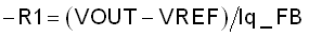
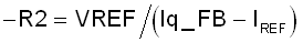
We might be able to increase the value ratio of R1- R2. However, system designers should consider noise immunity performance from the change and also, Compensation network will refer R1 into configuration.
Note, we will not discuss setting stability by compensation network. For detail information, see the Compensation Design with TL431 for UCC28600 application note.