SLVAF64A July 2021 – November 2022 TPS62800 , TPS62801 , TPS62802 , TPS62806 , TPS62807 , TPS62808 , TPS62864 , TPS62865 , TPS62866 , TPS62867 , TPS62868 , TPS62869 , TPSM82810 , TPSM82813 , TPSM82816 , TPSM82864A , TPSM82866A , TPSM82866C , TPSM8287A06 , TPSM8287A10 , TPSM8287A15 , TPSM8287B15 , TPSM8287B30
1 Introduction
Today, more and more engineers are asking for smaller components when designing their systems.
Smaller parts lead to a reduced board size, with the benefit of space critical applications (wearables, personal electronics, and so on) and reducing the cost.
Also, more devices can be incorporated on the same boards, leading to an increased complexity and additional capabilities per board area.
In the past, power managements DC-DC Buck ICs had an independent pin for every function, as power good, output voltage setting, mode of operation, and so on.
This limitation led to an intrinsic tradeoff; for space critical applications, the designer had to choose the simplest component, without any additional features, to assure the smallest package possible. For more complex designs, where more features are required, the only choice were bulky components with a big package and an elevated number of pins.
To overcome this tradeoff, Multi-function pins were introduced. A Multi-function pin is simply a single pin where more than one features are integrated.
This application note considers the TPS6280x, TPS6286x and TPSM8286xA family, that are capable of offering many features in a small size package.
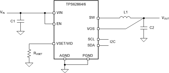
With this intent, an input pin is multiplexed to provide two different functions (VSET/VID for TPS62864/6/8/9, VSET/MODE for TPS62865/7 and TPSM82864/6A and VSEL/MODE for TPS62800/1/2/6/7/8), usually separated in time domain as shown in Figure 1-1.
 Figure 1-1 TPS62864/6 Typical Application
Schematics
Figure 1-1 TPS62864/6 Typical Application
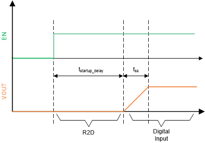
SchematicsAt the beginning, directly after enabling the startup (t_startup_delay), the ICs use the multiplexed pin for resistance measurement (R2D conversion, see Benefits of a Resistor-to-Digital Converter in Ultra-Low Power Supplies for reference), where the result allows to correctly set the output voltage value. During operation, the pin acts as a digital input as shown in Figure 1-2, to correctly configure the corresponding setting.
 Figure 1-2 VSET/MODE Pin Time Multiplexing
This application note describes the Multi-function pin behavior and it proposes some driving circuitry to effectively multiplex between the different features while avoiding measurement errors.