SLVAF83 August 2021 TPS23730
2 Layout Review Process
Please use the following the steps when reviewing the first revision of a layout, and then make changes accordingly.
- Locate Major Components*
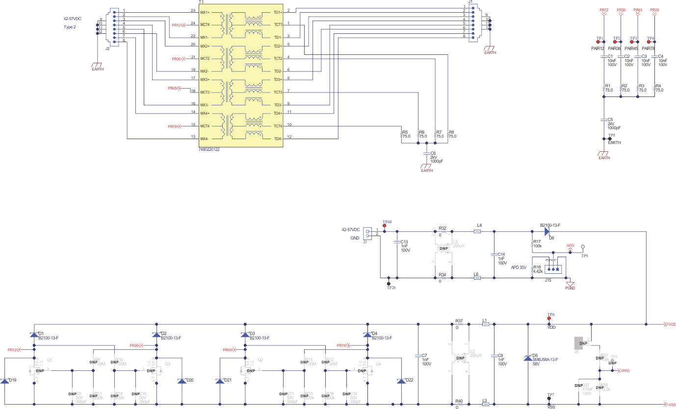
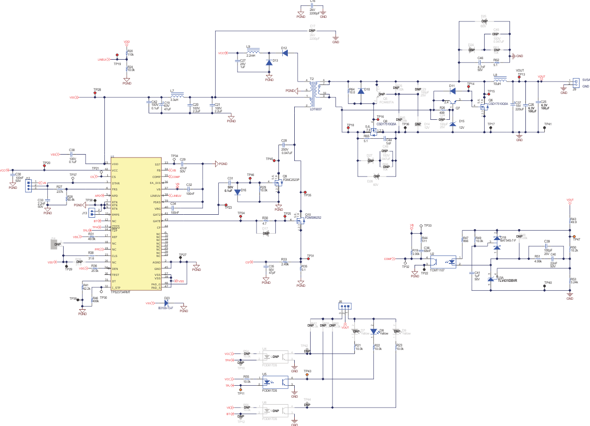
Use Figure 2-1 and Figure 2-2 for reference:
- Main DCDC Power Transformer (T2)
- IC (U1)
- RJ45 Jack (J1)
- Primary FET (Q2)
- Bulk Cap (electrolytic, C12)
- Primary Ground (PGND)
- VSS Plane (VSS)
- Secondary Ground
(GND).Note: *The schematic used here is the TPS23731EVM-095
 Figure 2-1 PoE PD Schematic
Input
 Figure 2-2 PoE PD Schematic Power
Stage
 - Determine if components are on the top side or bottom side or both
- Turn on only the top layer, and try to find the IC. Then turn on the bottom layer and determine if any components are there also.
- Cycle through the inner signal and ground layers – determine how many layers are dedicated to ground (primary, secondary, VSS). Also determine if any major signals (GATE, VCC, and so on) are carried on a different layer.
- There should be at least one layer completely dedicated to ground (if design is two layers). Most designs are more layers than this, and therefore there should be more layers with ground signals. For example, a four-layer design should have two layers dedicated to ground.
- Any unused space in a layer should be filled with a ground plane – so most of the design is a few big ground planes
- These ground layers should be stitched together with vias throughout and on the edges.
- Ensure that the Bob-Smith plane, VSS plane, primary ground plane and secondary ground plane do not overlap one another. Although they will not be connected electrically because they are on different layers, from an EMI perspective they will be shorted together and that can cause EMI noise.
- Locate input rectifier bridge (Diode, FET, integrated)
- Determine if there is an adequate Bob-Smith plane, with lines properly terminated. Please note that not all designs use a dedicated Bob-Smith plane; often it is connected to the secondary ground. For more information on the Bob-Smith plane, please see Practical Guidelines to Designing an EMI Compliant PoE Powered Device with Isolated Flyback.
- This can be relatively further away from the IC and DCDC
- Follow the rectified power signal (PoE+ and PoE-) to the input capacitors (C9 and C23), ferrite beads (L6 and L8), and EMI choke (L7).
- Ensure that there is no copper underneath the common mode choke or ferrite beads. This filter should provide isolation between the Bob-Smith plane and the primary ground.
- These components can also be somewhat further from the IC.
- EMI chokes are good for lower frequency EMI (reducing the common mode current)
- Ferrite beads are better for high frequency EMI
- Keep at least placeholders for these parts
- Find the TVS diode (D12) and 0.1uF bypass capacitor (C30) for VDD-VSS.
- Ensure these are as close to the IC as possible. Long traces create a parasitic inductance which reduces the ability of the diode to clamp at the correct voltage. The TVS diode protects the IC from overvoltage events, such as surge and ESD, so it is critical that it is close to the IC.
- The TVS needs a lot of vias to connect the different ground layers together.
- Follow the VDD line to the IC. Locate the detection resistor. This should be close to the IC. The following components should be close to the IC (and typically on the same side). This is critical since these signals are precision signals (vs the power path). So, their voltage/resistance is critical to be accurate, therefore they need to be close to the IC to mitigate the chance for any noise:
- DT resistor
- BLNK resistor
- FRS resistor
- PPD or APD divider
- V_REFF resistor (if applicable)
- CLS (A and B) Resistor- this has priority level two. Set the components above first, then set the CLS resistors as close as possible after that.
- If there is a TVS between VSS_RTN, this should be directly under the IC
- Next, it is easiest to check the other side of the controller for close components. By other side, I mean components that connect to RTN or GND (and sometimes are on the other side of the IC package). The following components should be close to the pins:
- VC bypass cap (0.1uF)
- VB bypass cap
- CS circuitry
- VBG (if applicable)
- SST (if applicable)
- I_STP (if applicable)
- Ensure the IC has vias to ground (and VSS) to ensure a good connection
- Find the bulk cap and input filter. The bulk cap needs to be close to the IC as well. After all the above components are set, then place the bulk cap close to the IC. This needs a lot of vias to connect to ground.
- Check the VC connection to the transformer. It does not need to be close to the IC, but ensure it does not directly cross critical signal paths if possible. Use a thicker trace here to provide a low inductance path for the power.
- Check the GATE path to the MOSFET. Attempt to make it as short as possible – this is very noisy. However, it is a secondary concern compared to the primary power path discussed below. A longer gate path can be acceptable if it is sandwiched between grounds. This means it is in an inner layer with a ground plane on both sides, that is well stitched together with vias. Additionally, the path must be wide enough to keep the inductance low. Wide enough will depend on the length of the signal, but the key is to not use the smallest trace possible. The other key with the gate path is to not run any other signals in parallel. For example, the feedback from the optocoupler, or the signal fed to CS should not be in parallel with this gate drive path.
- Find the primary MOSFET (s). Ensure they are as close to the transformer as possible. This is critical. Then look at the sense resistor ( the big one connected to the source of the FET, connecting to CS (current sense), usually is is <1ohm, R18). Additionally, the input ceramic capacitors (C13 and C14) should be included in this loop.
- This loop needs to be as tight as possible. This is the main power path. It is the highest Dv/Dt in the entire design. So it is the noisiest and will have the most thermal dissipation.
- The drain should have a copper plane to dissipate heat. But it also acts like an antenna, so the bigger the copper, the worse the EMI performance. This is a design trade-off the designer needs to make. The designer can use multiple layers and layer in ground layers for the FET to minimize the EMI while maximizing the amount of copper to dissipate heat.
- Gate drive components (resistors, BJTs, diodes), need to be as close to the FET as possible as well.
- The sense resistor should have lots of vias to ensure a good ground connection.
- The ground of the ceramic capacitors should be very close to the ground of the sense resistor. This makes the loop very tight.
- Put many vias on the VDD pin of the transformer (pin 2 of T2). It is suggested to put at least 6 vias here in order to help with transformer thermal dissipation.
- Look at the common mode capacitors (C28 and C11) between primary and secondary ground. These should be underneath the transformer. They should set the isolation barrier – meaning pull the ground plane up to the capacitor pad, but use the dielectric spacing to be the spacing between the ground planes. Every single cap needs at least two vias on both sides to ensure good ground connections. The purpose of these capacitors is to short out the trace capacitance of the DCDC transformer. This trace capacitance creates an unwanted common mode current path that enables ESD and surge currents, as well as EMI noise, to travel across the isolation barrier. So the common mode capacitors provide a known path for all of these signals. Therefore, it is suggested to place them as close to or under the transformer as possible. It is also suggested to connect them to large ground planes with vias to dissipate these signals with minimal impedance. It is suggested to have at least two capacitors underneath the transformer.
- Move on to the secondary. This will depend heavily on the topology. But the basic rules are:
- The switching components (MOSFET or diode) need to be as close to the transformer as possible. Associated snubbers or gate drive circuits needs to be close as well. This is the main power path, and the loop should be as tight as possible. Prioritize MOSFET or diode placement, then the snubber, and then the gate drive components.
- Use planes for cathodes, anodes, sources and drains. This is the main power path – give the current lots of copper to flow through to minimize thermals but not too much because of EMI. These planes should be multilayered and have vias. Heat comes off of the cathode of a diode, so it is advantageous to have the cathode connect to a large plane with vias. This comes down to if the diode is connected to the high side or low side of the transformer. Essentially, the cathode should be on the output side and the anode should be on the switching side connected to the transformer. This is called high side. Low side would have the anode connected to ground, and cathode connected to the transformer. This creates an unnecessary trade off between thermals and EMI. The same principle is true for MOSFETs. The drain of a MOSFET dissipates the heat, so we want the drain on the output side. However, in topologies such as active clamp forwards, connecting the drain of the MOSFETs to the switching node is unavoidable, and the thermal/EMI tradeoff will have to occur.
- The ground pin of the transformer should have many vias connected to it. It is suggested to have at least 6 vias; this is for the transformer thermal performance.
- The optocoupler and feedback circuitry should be on the side of the transformer, away from the main power path. This is a critical signal, so keep it electrically away from the main power path that is switching. Using ground planes to sandwich the signal is considered best practice, but as long as the noise from the switching components is not directly over the feedback lines this should be acceptable. The feedback components (capacitors, resistor and shunt voltage regulator), should be as close to the optocoupler as possible. The resistor divider that is connected to the reference pin of the shunt regulator should be very close to the reference pin. Make the entire feedback network tight as possible.
- The filter on the primary side of the optocoupler (on VB and CTL), should be either close to the IC or close to the optocoupler. Both versions have been tested, and do not significantly impact the EMI performance. However, the components should be close to one or the other. As stated previously, this primary feedback trace should not run in parallel with the primary MOSFET gate drive trace. It should also avoid the primary MOSFET switching node, as this signal is small compared to the primary power.