SLVAFC5 March 2022 TPS629210 , TPS629210-Q1
5 How to Modify a Buck to Inverting Buck-Boost?
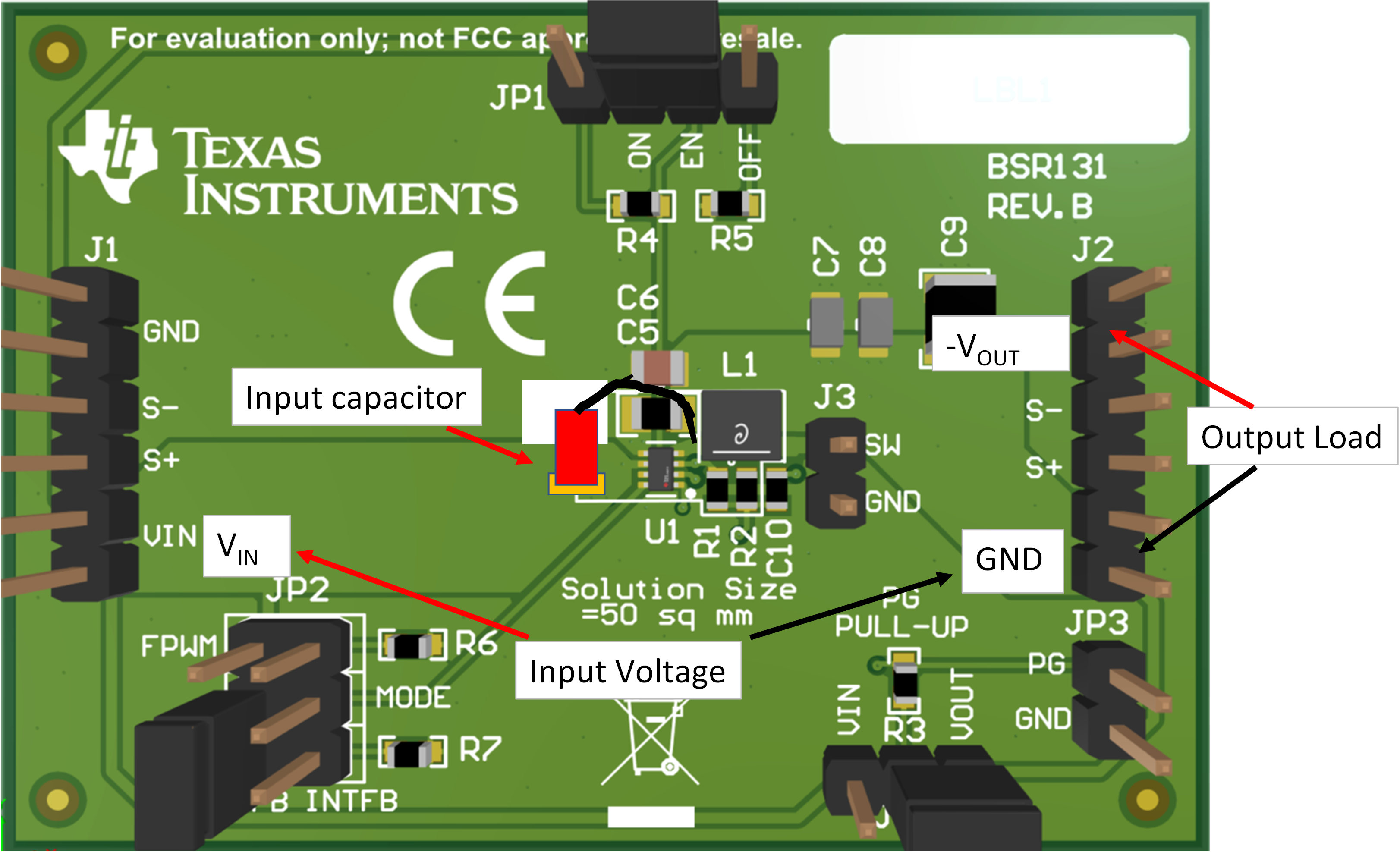
To achieve the inverting function, the output terminals are swapped such that VOUT becomes GND and the GND terminal becomes -VOUT. Everything was GND is now labeled - VOUT. The modification shown in .Figure 5-1
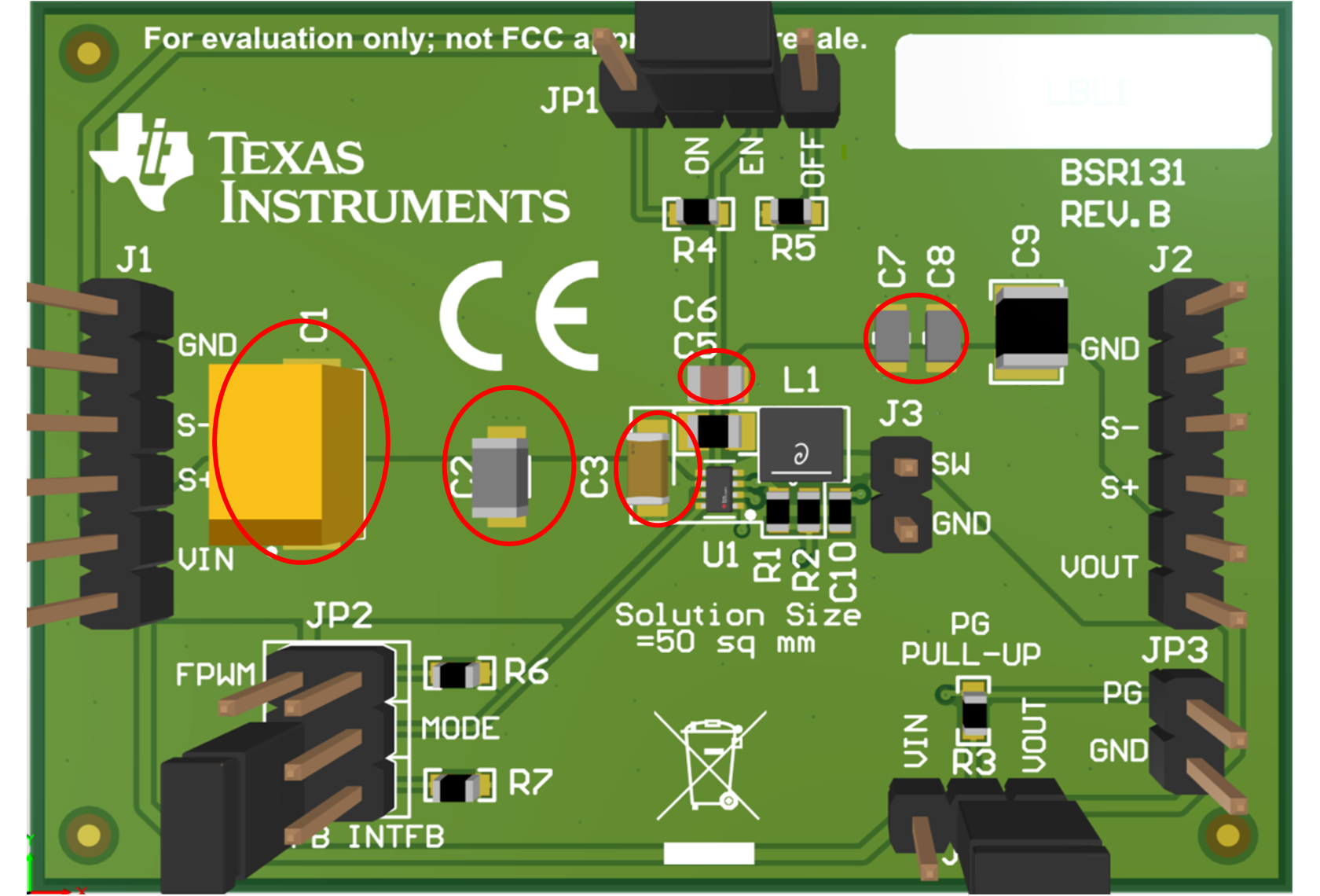
- The reference designators are identical between buck and inverting buck boost, except for the input capacitors C1, C2 and C3 whose connections need to be changed
- Remove input capacitor C1, C2 and C3 from the EVM, but save them to re-install later
- Install 2 pcs 22 μF, 10V ceramic output capacitors at C6 and C7. Might add more to reduce output ripple and improve loop stability.
- Change the value of R1 and R2 to set the appropriate output voltage
 Figure 5-1 Buck EVM Before Modification
- Because existing input GND pads of input capacitors C3 are not the correct electrical location on existing EVM. So put a electrical tape to cover that GND pad of C3 to avoid wrong connection.
- The existing pad for VIN connection of C3 is used and a wire is added to complete the connection to GND, which is Vout on the PCB
- Re-install C1, C2 and C3 as highlighted in red square area
- Input supply can be applied between VIN and GND, which is VOUT on the PCB
- Load can be applied between -VOUT and GND
 Figure 5-2 Inverting Buck-Boost EVM After
Modification