SLVAFP1 February 2024 TPS54KB20
5 Test Data
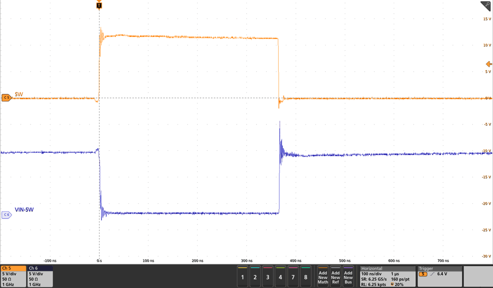
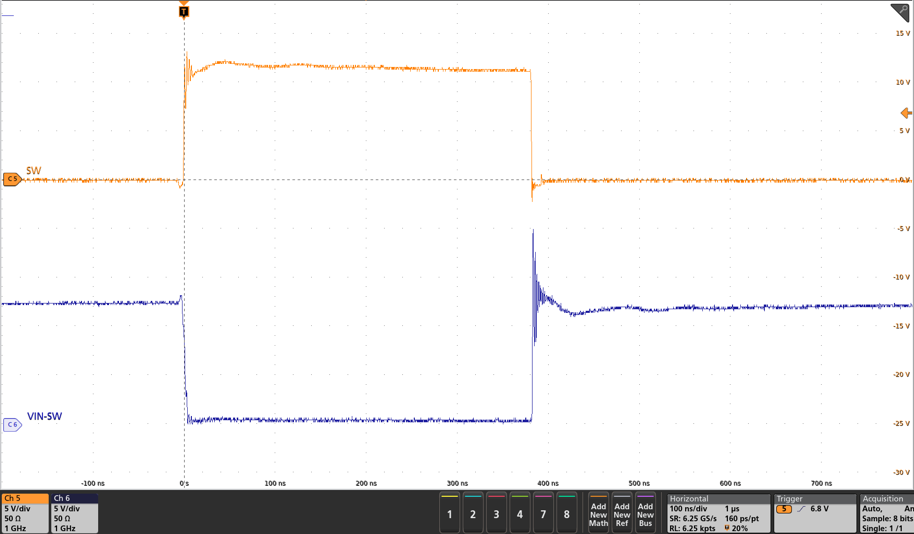
The experimental data below displays a waveform comparison between the two footprints, showing SW-node and VIN-SW signals. The data is measured at 12V Vin, 3.3V Vout, 25A load, and internal VCC.
 Figure 5-1 Symmetrical Footprint
SW-Node and VIN-SW
 Figure 5-2 Asymmetrical Footprint
SW-Node and VIN-SW
Figure 5-2 Asymmetrical Footprint
SW-Node and VIN-SWSymmetrical bench data, Figure 5-1, and Asymmetrical bench data, Figure 5-2, are compared to reflect the difference in SW-node ringing when tested under identical parameters.
Figure 5-3 compares efficiency data between the symmetrical and asymmetrical layout.
 Figure 5-3 Efficiency (Vin = 12V, 800 kHz
FCCM)