SLVUA04A February 2014 – January 2022 LMZ31704 , LMZ31707 , LMZ31710
2 Getting Started
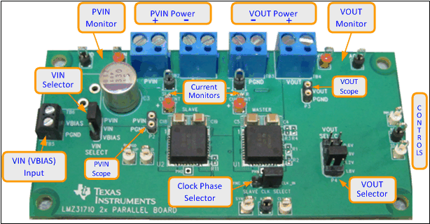
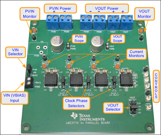
Figure 2-1 and Figure 2-2 highlight the user interface items associated with both the 2× and 4× LMZ31710 parallel test board. The polarized PVIN power terminal blocks are used to connect to the host input supply, and the polarized VOUT power terminal blocks are used to connect to the load. These terminal blocks can accept up to 16 AWG wire. The polarized VBIAS terminal block is used along with the VIN SELECT jumper (P1) when optional split power supply operation is desired. Refer to the LMZ31710 10-A Module, 2.95-V to 17-V Input and Current Sharing in QFN Package data sheet for further information on split power supply operation. Refer to Table 2-1 for terminal block numbering for either the 2× or 4× LMZ31710 parallel test board.
 Figure 2-1 2×
LMZ31710 Test Board User Interface
 Figure 2-2 4×
LMZ31710 Test Board User Interface
Figure 2-2 4×
LMZ31710 Test Board User Interface| Function | 2× LMZ31710 | 4× LMZ31710 |
|---|---|---|
| PVIN Power | TB1 | TB1 |
| PGND (Input) | TB2 | TB2 |
| PGND (Output) | TB3 | TB3, TB4 |
| VOUT Power | TB4 | TB5, TB6 |
| VBIAS Input | TB5 | TB7 |
The PVIN monitor and VOUT monitor test points located near the power terminal blocks are intended as voltage monitoring points where digital voltmeters can connect to measure PVIN and VOUT.
Do not use these PVIN and VOUT monitoring test points as the input supply or output load connection points. The PCB traces connecting to these test points are not designed to support high currents. High currents can damage the PCB traces.
The PVIN Scope and VOUT Scope test points can be used to monitor PVIN and VOUT waveforms with an oscilloscope. These test points are intended for use with un-hooded scope probes outfitted with a low-inductance ground lead (ground spring) mounted to the scope barrel. The two sockets of each test point are on 0.1-inch centers. The scope probe tip should be connected to the socket labeled PVIN, or VOUT, and the scope ground lead should be connected to the socket labeled PGND.
The current monitor test points located above each LMZ31710 device are intended to be used with digital voltmeters to monitor the current across a 1-mΩ sense resistor located on the bottom of the board. The controls test points located on the perimeter of the board are made available to test the features of the device. Any external connections made to these test points should be referenced to an AGND test point. Refer to Section 3 for more information on the individual control test points.
The VOUT SELECT jumper (P4) is provided for selecting the desired output voltage. Before applying power to the test board, ensure that the jumper is present and properly positioned for the intended output voltage. Always remove input power before changing the jumper settings.