SLVUCB9 October 2021
4 PCB Layout
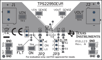
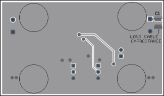
Figure 4-1 and Figure 4-2 show the PCB layout images.
 Figure 4-1 TPS22950LEVM Top Layout
 Figure 4-2 TPS22950LEVM Bottom Layout
SLVUCB9 October 2021
Figure 4-1 and Figure 4-2 show the PCB layout images.
 Figure 4-1 TPS22950LEVM Top Layout
 Figure 4-2 TPS22950LEVM Bottom Layout