SLVUCL3 December 2022
- Abstract
- Trademarks
- 1Cautions and Warnings
- 2Introduction
- 3Quick Start Guide
- 4Hardware and Software Overview
- 5Hardware Setup
- 6Firmware and GUI Application
- 7Schematics
- 8Revision History
4.4 DRV8317HEVM Configurability – Jumpers and Resistors
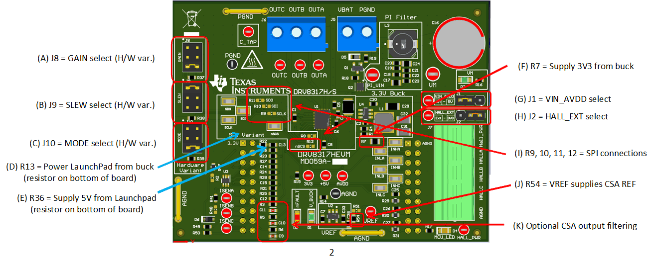
The DRV8317HEVM includes a variety of user-selectable jumpers and unpopulated components on the PCB to choose user settings and evaluate the DRV8317H or the DRV8317S device. A summary of those selectable settings is listed in Table 4-2 (defaults in bold), and can be seen on the board in Figure 4-5. Section 4.4.2 describes the changes that need to be made to the board in order to use the SPI variant as the main motor driver IC.
Id. | Setting Name | Description | Position | Function |
|---|---|---|---|---|
A | GAIN select | (DRV8317H only) Use J8 to select desired gain settings. DNP jumper if DRV8317H is not used. | J8 = Bottom | 0.25 V/A |
J8 = Middle | 0.5 V/A | |||
J8 = No Jumper | 1 V/A | |||
J8 = Top | 2 V/A | |||
B | SLEW select | (DRV8317H only) Use J9 jumper to select desired slew rate settings. DNP jumper if DRV8317H is not used. | J9 = Bottom | 25 V/us |
J9 = Middle | 50 V/us | |||
J9 = No Jumper | 125 V/us | |||
J9 = Top | 200 V/us | |||
C | MODE select | (DRV8317H only) Use J10 jumper to select desired PWM mode. DNP jumper if DRV8317H is not used. | J10 = Bottom | 6x PWM mode |
J10 = Middle | 6x direct PWM mode | |||
J10 = No Jumper | 3x PWM mode | |||
J10 = Top | 3x direct PWM mode | |||
D | Power LaunchPad from buck | 0-ohm R13 resistor on bottom of board used to supply power from buck to LaunchPad. DNP if powering LaunchPad externally. See Section 4.4.3 on MCU Power | See Section 4.4.3 on MCU power options | |
E | Supply 5 V from LaunchPad | 0-ohm R36 resistor on bottom of the board Supplies 5 V from the F280049C LaunchPad boost converter. | R36 is populated | Supply 5 V from LaunchPad |
R36 is DNP | Supply 5 V externally (if desired) from the+5V test point | |||
F | Supply 3.3 V from buck | 0-ohm R7 resistor connects buck 3.3 V voltage to supply main 3.3 V. | R7 is populated | Connects buck output to supply 3.3 V rail |
R7 is DNP | Supply 3.3 V externally from the 3V3 test point | |||
G | VIN_AVDD select | Use J1 to supply VIN_AVDD voltage from either VM or 5 V. | J1 = Left | VIN_AVDD supplied from VM |
J1 = Right | VIN_AVDD supplied from 5 V | |||
H | HALL_EXT select | Use J2 to supply Hall power externally or from 3.3 V | J2 = Left | Hall power supplied externally from the HALL PWR test point |
J2 = Right | Hall power supplied from 3V3 | |||
I | SPI variant connections | Populate specific resistors to properly use the Hardware or SPI variant | SPI variant: Populate R9, R10, R11, and R12 | |
J | VREF connection | 0-ohm R54 resistor supplies CSA REF from on-board VREF | R54 is populated | CSA REF is supplied from on-board VREF voltage |
R54 is not populated | CSA REF needs to be supplied externally through VREF test pin | |||
K | CSA output filtering | C9-11 and R3, 5, and 6 are used for RC filtering | C9-11 and R3, 5, and 6 populated | RC filter for CSA outputs |
| C9-11 and R3, 5, and 6 not populated | No RC filter for CSA outputs |
 Figure 4-5 User-selectable jumpers and DNP components on DRV8317HEVM