SNAA285 October 2015 LMK61E2
1
When measuring jitter performance of oscillators, it is important to understand the limitations of the measurement equipment used. This application note will primarily focus on highlighting some of the limitations of real-time oscilloscopes used for time-domain jitter analysis.
Time-domain jitter specifications of interest are period jitter, cycle-to-cycle jitter, time interval error (TIE) and Total Jitter (TJ).
Per JEDEC Standard JESD65B, period jitter is defined as the deviation in cycle time of a signal with respect to the ideal period over a random number of cycles. The number of cycles selected for this measurement should be significant (1000 to 10,000) to have sufficient confidence in the measurement. Peak-to peak period jitter is defined as the difference between the largest and the smallest period value from the sample size used for the measurement. Period jitter can also be specified as a root means squared (RMS) value in lieu of peak-to-peak. This jitter specification is primarily used for guaranteeing setup and hold times for logic in CPUs and FPGAs.
Cycle-to-cycle jitter is defined as the variation in cycle time of a signal between adjacent cycles over a random sample of adjacent cycle pairs. Once again, the number of cycles selected for this measurement should be significant (1000 to 10,000) to have sufficient confidence in the measurement. Cycle-to-cycle jitter is typically specified as the greater of the absolute values of the worst case positive or negative variation in cycle time between adjacent cycles. As an example, if the largest positive cycle-to-cycle variation is 62ps and the largest negative cycle-to-cycle variation is -65ps, the overall cycle-to-cycle jitter is commonly specified to be 65ps.
TIE, also known as accumulated jitter is the deviation of a clock period from the ideal clock period measured over a significant number of cycles. It includes jitter contribution due to high and low jitter modulation frequencies. This specification of jitter is commonly used in SONET and Optical Transport Networking (OTN) equipment.
Total Jitter (TJ) is another time-domain jitter specification commonly used in Serial IO applications that is derived from the TIE measurement. It is measured at a specified Bit Error Rate (BER) for the serial IO link and combines the effect of Random and Deterministic jitter components. It predicts a peak-to-peak jitter that will only be exceeded with a probability equal to the BER. Real-time oscilloscopes typically include jitter analysis software tools that decompose TJ into random (RJ) and deterministic jitter (DJ) components. The relationship between TJ, RJ and DJ is shown in Equation 1.

- n is the application BER multiplier
where
Table 1 gives a complete list of multipliers for required BER.
Table 1. BER Multipliers
| BER | Multiplier |
|---|---|
| 10-3 | 6.582 |
| 10-4 | 7.782 |
| 10-5 | 8.834 |
| 10-6 | 9.784 |
| 10-7 | 10.654 |
| 10-8 | 11.462 |
| 10-9 | 12.218 |
| 10-10 | 12.934 |
| 10-11 | 13.614 |
| 10-12 | 14.260 |
| 10-13 | 14.882 |
| 10-14 | 15.478 |
| 10-15 | 16.028 |
The jitter specifications described above were measured using a real-time digital phosphor oscilloscope from Tektronix (DPO70804C) on a 312.5 MHz output frequency clock generated using the LMK61E2 high performance programmable oscillator from Texas Instruments. The measurement results are shown in Figure 1.
 Figure 1. Time-Domain Jitter Measurement Results
 The sample size for the above measurements was > 10000 samples and the sampling rate was set to 25GS/s (maximum allowable sampling rate for the oscilloscope). The acquisition interval for the measurement was 40us. A Bit Error rate of 1E-12 was selected for the Total Jitter (TJ) measurement and a 20 MHz low pass filter was applied to the TIE, TJ, RJ, and DJ measurements.
Jitter measurements on real-time oscilloscopes are affected by factors inherent to the oscilloscope. The major sources of noise within the oscilloscope are sampling jitter, vertical noise, timing stability and signal interpolation error.
Signal interpolation error due to linearly interpolating between voltage samples can be minimized by using sin(x)/x (or sinc) interpolation setting on the oscilloscope (if available) and by maximizing signal amplitude to input full scale.
Vertical noise in an oscilloscope is intrinsic to the input attenuators, preamplifiers and A/D converters. This noise varies with the front-end attenuator and amplifier settings, bandwidth limiting on the scope and sample size used for the measurement. Oscilloscope user manuals specify the vertical noise at a particular V/div setting or as a percentage of the V/div setting.
Timebase stability is another potential source of error in real-time oscilloscopes. The timebase stability is usually specified in the oscilloscope datasheets. ADC aperture uncertainty and quantization error are other sources of error in the oscilloscope that manifest as amplitude and timing noise.
The slew rate of the signal being measured affects the jitter. If the edge rate of the signal measured is slow relative to the system bandwidth, any amplitude noise at the threshold crossing of the signal can result in increased jitter. Slew rate amplifiers can potentially be used to increase the slew rate of the signal before it is connected to the oscilloscope. In general, the faster the edge rate of the signal being measured, the lower will be the impact of any amplitude noise. The use of a limiting amplifier (ONET1191P) for total jitter measurement has been covered in detail in the applications note SCAA120A from Texas Instruments. It should be noted that any limiting amplifier or slew rate amplifier device will contribute some additive jitter to the signal being measured. Also, for measuring signals with fast slew rates, an oscilloscope with adequate sampling rate should be used. The measurements in this application note were not made using any limiting amplifiers or slew rate amplifiers.
The above sources of error are factored in a parameter called JNF for the Tektronix DPO70804C real-time oscilloscope. Jitter Noise Floor is defined as the intrinsic noise portion of a jitter measurement. This sets the lower limit on the amount of jitter that the oscilloscope can detect. If the input signal has jitter lower than the jitter noise floor of the oscilloscope, the measured jitter on the oscilloscope will not accurately represent the true jitter of the input signal.
JNF is described in Equation 2 (referred from Tektronix application note 61W_18786_2).
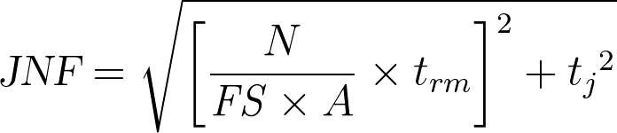
- A = input signal amplitude (volts)
- trm = 10% to 90% measured rise time (sec)
- FS = full scale range of input
- tj = short/medium term aperature uncertainty (sec rms)
- N = input-referred noise (volts rms)
where
The details of this specification are beyond the scope of this application note.