SNAA291A May 2016 – April 2021 ADC32RF45 , LMX2582 , LMX2592
4 Factors Influencing Jitter
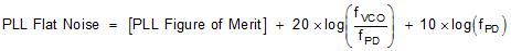
A phase noise of a synthesizer is mainly a combination of the Phase Locked Loop (PLL) and the Voltage Controlled Oscillator (VCO). The specification on datasheets that can tell you how low a jitter you are capable of achieving is the Normalized PLL Noise Floor (PLL Figure of Merit), Normalized PLL Flicker Noise (changes by 10 dB / dec), and VCO open-loop phase noise in data sheets. The PLL Figure of Merit and Flicker Noise are described in Equation 3 and Equation 4. From the relation seen in Equation 3, you can see that doubling fPD essentially decreases the [20 × log] component by 6 dB and increases the [10 × log] component by 3 dB, so in total the overall PLL flat noise decreases by 3 dB. This is one of the aspects that improve the phase noise contributed by the PLL.
where
- fPD is the phase detector frequency of the synthesizer
- fVCO is the voltage controlled oscillator frequency

In Figure 4-1, the black line is the original phase noise with a 58 fs jitter. But if the PLL phase noise is worse, as seen in the raised flat portion of the red line, the jitter can go up (78 fs in this example). The VCO phase noise also makes a big difference. Observe the gray line, a degraded VCO phase noise in this case, increased the jitter to 110 fs. By choosing a device that has good performance in both these areas and then designing the loop filter of the synthesizer well for the best phase noise response around the loop bandwidth, the lowest jitter can be optimized, providing the highest SNR clocking for the ADC.
 Figure 4-1 Phase
Noise Contribution from PLL and VCO
Figure 4-1 Phase
Noise Contribution from PLL and VCOThere are also considerations for improving the jitter of the synthesizer in the signal amplitude, which affects the noise floor and thus the jitter caused by higher offsets. This behavior is observed through Leeson’s equation, where the phase noise level floor level changes by output power with a factor (1 / Ps) of the signal source. At some point, the noise floor of the clock source will dominate and there is no further improvement (around 0 dBm from Figure 4-2). The clock source amplitude should be designed to be at least this level. Consequently, a synthesizer device with a very low noise floor as well as the capability of higher output power to reach this noise floor level is desired. As discussed in the earlier section of integration range for jitter, the higher the upper range, the more of this high offset phase noise will influence the overall jitter.
 Figure 4-2 Sampling Clock Amplitude