SNAU263A February   2022  – July 2022


  1.   Abstract
  2.   Trademarks
  3. 1Introduction
  4. 2EVM Quick Start
  5. 3EVM Configuration
    1. 3.1  Power Supply
    2. 3.2  Logic Inputs and Outputs
    3. 3.3  Switching Between I2C and SPI
    4. 3.4  Generating SYSREF Request
    5. 3.5  XO Input
      1. 3.5.1 48-MHz TCXO (Default)
      2. 3.5.2 External Clock Input
      3. 3.5.3 Additional XO Input Options
      4. 3.5.4 APLL Reference Options
    6. 3.6  Reference Clock Inputs
    7. 3.7  Clock Outputs
    8. 3.8  Status Outputs and LEDS
    9. 3.9  Requirements for Making Measurements
    10. 3.10 Typical Phase Noise Characteristics
  6. 4EVM Schematics
    1. 4.1  Power Supply Schematic
    2. 4.2  Alternative Power Supply Schematic
    3. 4.3  Power Distribution Schematic
    4. 4.4  LMK5B33216 and Input Reference Inputs IN0 to IN1 Schematic
    5. 4.5  Clock Outputs OUT0 to OUT3 Schematic
    6. 4.6  Clock Outputs OUT4 to OUT9 Schematic
    7. 4.7  Clock Outputs OUT10 to OUT15 Schematic
    8. 4.8  XO Schematic
    9. 4.9  Logic I/O Interfaces Schematic
    10. 4.10 USB2ANY Schematic
  7. 5EVM Bill of Materials
    1. 5.1 Loop Filter and Vibration Nonsensitive Capacitors
  8. 6Appendix A - TICS Pro LMK5B33216 Software
    1. 6.1  Using the Start Page
      1. 6.1.1 Step 1
      2. 6.1.2 Step 2
      3. 6.1.3 Step 3
      4. 6.1.4 Step 4
      5. 6.1.5 Step 5
      6. 6.1.6 Step 6
      7. 6.1.7 Step 7
    2. 6.2  Using the Status Page
    3. 6.3  Using the Input Page
      1. 6.3.1 Cascaded Configurations
        1. 6.3.1.1 Cascade VCO to APLL Reference
    4. 6.4  Using APLL1, APLL2, and APLL3 Pages
      1. 6.4.1 APLL DCO
    5. 6.5  Using the DPLL1, DPLL2, and DPLL3 Pages
      1. 6.5.1 DPLL DCO
    6. 6.6  Using the Validation Page
    7. 6.7  Using the GPIO Page
      1. 6.7.1 SYNC/SYSREF/1-PPS Page
    8. 6.8  Using the Outputs Page
    9. 6.9  EEPROM Page
    10. 6.10 Design Report Page
  9. 7Revision History

Step 3

Set the clock input select mode for the DPLLs, input priority, and maximum TDC frequency. The recommended Input Select Mode is Auto Revertive. REF0 and REF1 shown below correspond with IN0 and IN1, respectively. REF4 and REF5 priorities can be set if the DPLLs input will be fed from one of the APLL post divider frequencies. The corresponding APLL is listed next to the REF4 and REF5. The REF with the highest priority will be fed as the DPLL input.
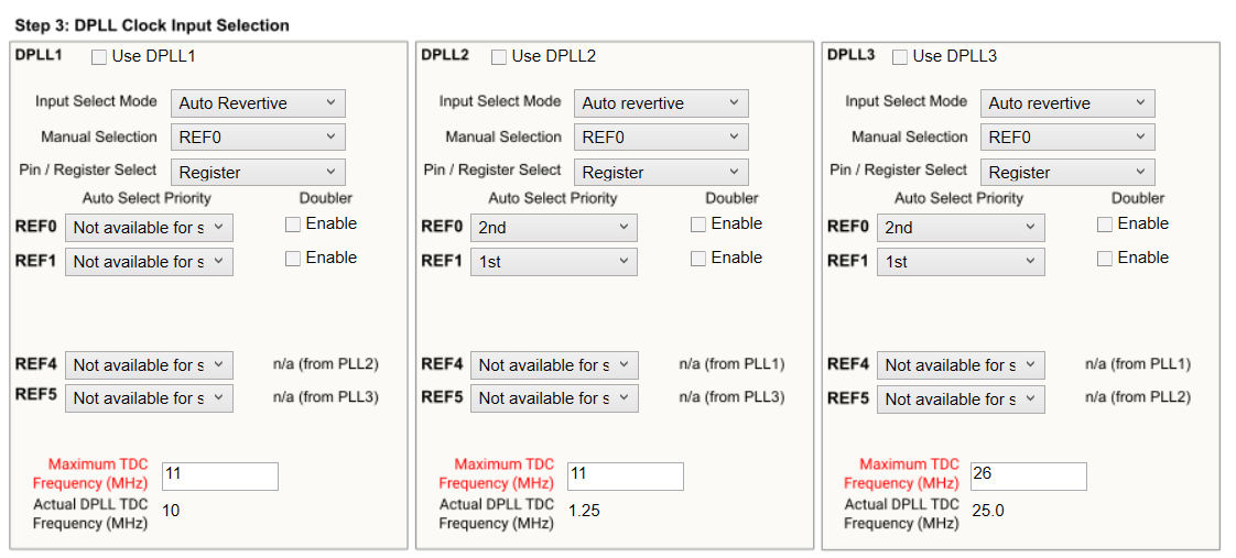
GUID-20211204-SS0I-GKCN-6BRB-HTJBHDPFVSLC-low.pngFigure 6-3 Step 3: DPLL Clock Input Selection.