SNOU176B October 2020 – March 2022
PRODUCTION DATA
- Trademarks
- 1 General TI High Voltage Evaluation User Safety Guidelines
- 2 Introduction
- 3 LMG342XEVM-04X Schematic
- 4 Mother Board Schematic
- 5 Recommended Footprint
- 6 Test Equipment
- 7 Test Procedure When Paired With LMG342X-BB-EVM
- 8 Test Procedure When Paired With LMG34XX-BB-EVM
- 9 Bill of Materials
- 10Revision History
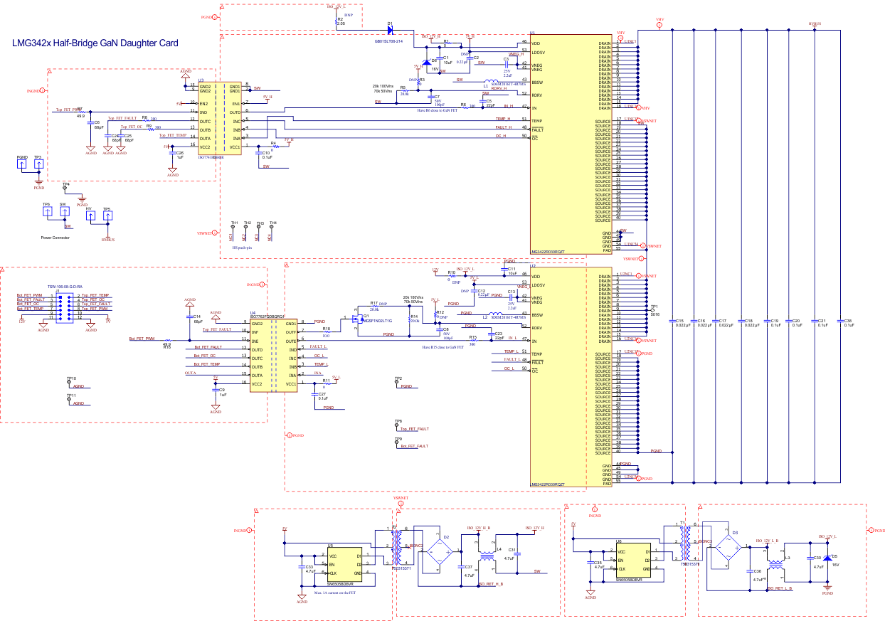
3 LMG342XEVM-04X Schematic
 Figure 3-1 LMG342XEVM-04X Schematic
Here are some of the guidelines while designing with LMG342x.
The ISO77xx series provides the best common-mode transient immunity capability. It is highly recommended to use ISO77xxF series which has default output as LOW in the case of carrier signal is affected by the common-mode noises, helping to avoid any shoot throughs for PWM signals. An RC filter is recommended on the isolator output for FAULT signal and OC signal in order to reduce teh CMTI noises. A 100 pF capacitor is recommended in parallel to the Rdrv resistors (R5 and R14) to mitigate the high-frequency noises coupled to slew-rate setting circuit.
Slew rate of the GaN device can be adjusted by changing the resistor connection at the RDRV pin. At very high slew rate operation (such as RDRV connected to GND), LDO5V pin may get overstressed due to ground bouncing. During such condition, it is recommended to remove capacitor closer to LDO5V (C2 and C12) and add a small resistor of 10 ohm (R4 and R11) between this pin and VCC of digital isolators. This helps in mitigating the over voltage stress on the LDO5V.
For the bootstrap power supply operation, a SiC Schottky diode (GB01SLT06-214) is recommended. The bootstrap resistance is suggested to be 2 Ω for high-frequency and low-duty cycle operations. Also, a large footprint SMD resistors with copper vias is preferred for thermal management. A 16V Zener diode needs to be placed close to the high-side Vdd pin. When bootstrap is used, the low-side GaN device’s slew rate needs to be controlled during the start-up. When the high-side power supply is fully charged, the low-side device can shift back to a higher slew rate in normal operation. This is realized using Q1 and R18. R14 of 100 kΩ is used to control the slew rate.