SNVA935A June 2020 – July 2021 LM60430 , LM60430-Q1 , LM60440 , LM60440-Q1
2.3 Enhanced HotRod QFN Pin-Out
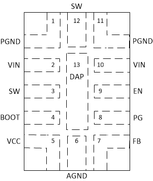
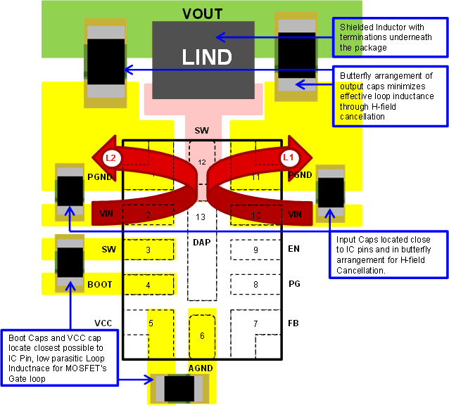
Another key feature for best-in-class EMI performance is the ability to optimize the pin-out. The optimized pin-out of the LM60440 device is shown in Figure 2-5. The LM60440 has parallel pins for the input power and GND pins which enables the symmetrical placement of high frequency input capacitors, and the equivalent parasitic loop inductance of the two equal, parallel inductances, is halved. Consequently, the circulating input currents create opposing magnetic fields that result in H-field cancellation and reduced radiated emissions. Furthermore, by performing the symmetric layout of the high di/dt input loops, the magnetic fields generated (of opposing directions) can cancel each other. To further reduce parasitic inductance place a continuous ground plane for return current underneath the L1 and L2 loops on layer 2 of the PCB - immediately below the top layer power circuit (Figure 2-8). Additionally the LM60440 device has conveniently routed the switch node pin internally. The second switch node pin is placed directly adjacent to the BOOT pin (boot-strap supply voltage for internal high-side driver). This simplifies routing the boot capacitor and reduces the SW area. The close placements of both the boot and VCC capacitors reduces the parasitic inductance for the gate driver circuitry and the commutating power loop carrying high-frequency currents during the MOSFET switching and ultimately reduces the conducted and radiated emissions.
 Figure 2-7 LM604x0 Pin-out
 Figure 2-8 LM604x0 Layout With Parallel Input Loops
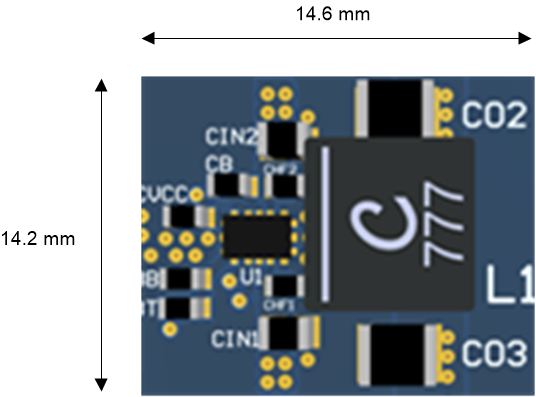
The optimized pin-out of the LM60440 allows for a dense layout and a compact total solution size (Figure 2-9).
 Figure 2-9 LM60440AQEVM Solution Size