SNVA962 December 2020 TPSM5601R5H
3.1 Additional Bypass Capacitor and Schottky Diode
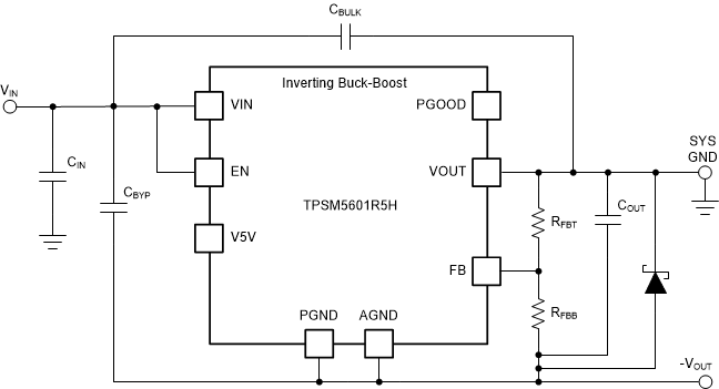
A ceramic bypass capacitor, CBYP, with a minimum capacitance of 10 µF is recommended to be placed from VIN to –VOUT. CBYP can help filter the input voltage and minimize interference with other circuits. The voltage rating of the capacitor must be taken into consideration because it will experience stress equal to the full voltage range between VIN and VOUT.
Consider that the inclusion of the bypass
capacitor introduces an AC path from VIN to VOUT and might worsen
the transient response. When VIN is applied to the circuit, this dV/dt
across CBYP creates a current that must return to ground to complete the
loop. This current might flow through the internal low-side body diode of the MOSFET and
inductor to return to ground. For this case, it is recommended to have a Schottky diode
between
–VOUT and SYS_GND as in Figure 3-1. If large-line transients are expected, increase the output capacitance to keep the
output voltage within acceptable levels.
It is also recommended that a capacitor, CBULK, is placed at the input power supply to help dampen the high-frequency noise that can couple onto the circuit. An electrolytic capacitor with moderate ESR helps dampen any input supply ringing caused by long power leads. When using the TPSM5601R5HEVM, adding a CBULK capacitor across VIN and SYS_GND is recommended.
 Figure 3-1 TPSM5601R5H Inverting Buck-Boost Schematic with Schottky Diode