SNVA962 December 2020 TPSM5601R5H
3.4 Power-Good Pin (PGOOD)
The TPSM5601R5H has a built-in power-good (PGOOD) function to indicate proper output voltage regulation. The PGOOD pin is an open-drain output that requires a pullup resistor. Because –VOUT is the return path of the IC in IBB topology, the PGOOD pin is referenced to –VOUT instead of system ground, which means that the device pulls PGOOD to –VOUT when it is low.
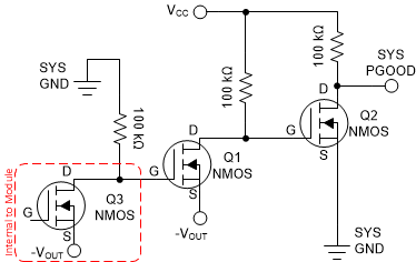
This behavior can cause difficulties in reading the state of the PGOOD pin, because in some applications the IC detecting the polarity of the PGOOD pin may not be able to withstand |–VOUT|. The level shifter circuit alleviates any difficulties associated with the offset PGOOD pin voltages by translating the negative output signals of the PGOOD pin. If the PGOOD pin functionality is not needed, it may be left floating or connected to –VOUT without this circuit.
 Figure 3-4 PGOOD Pin Level Shifter
Inside these devices, the PGOOD pin is connected to an N-channel MOSFET (Q3). By tying the PGOOD pin to the gate of Q1, when PGOOD is pulled low by the module, Q1 turns off and Q2 turns on because its VGS detects the VCC pull-up. Therefore, this pulls SYS_PGOOD to SYS_GND.
When Q3 turns off, PGOOD pin is pulled high (gate of Q1) to ground potential therefore turning it on. This pulls the gate of Q2 below ground, turning it off. SYS_PGOOD is then pulled up to the VCC voltage. Note that the VCC voltage must be at an appropriate logic level for the circuitry connected to the SYS_PGOOD net.