SNVU694A February 2020 – July 2020 LM76005 , LM76005-Q1
2.1 Input/Output (I/O) Connector Description
- VIN – Terminal on J1The power input terminal for the converter
- VOUT – Terminal on J2The regulated output voltage for the converter
- VIN_EMI – Terminal on J6Used to supply the input voltage through an on board LC filter (if one is needed for conducted
EMI/EMC measurement). The L1 and CBULK component
pads are located on the bottom side of the EVM.
Refer to Figure 3-1 for initial suggestion of
component values. J6 and LC filter are not
populated on this EVM.
- GND – Terminal on J1, J2 and J6The ground reference for the converter
- EN – TestpointUsed to enable the converter by supplying a voltage greater than 1.2 V (typ) or just to monitor the voltage on this pin whenever a resistor divider is in place (for precision enable applications). The regulator is enabled when VIN > 3.5 V. This threshold can be calculated by:
Equation 1. 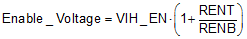
- PG – TestpointUsed to monitor the power-good flag. This flag indicates whether the output voltage has reached its regulation point. This pin is an open-drain output that requires a pullup resistor to the appropriate logic voltage (any voltage less than 20 V).
- PG_PU – TestpointThe top connection of an optional 100-kΩ pullup resistor that ties directly to the open-drain PG
pin. Supply an appropriate voltage to this test point, or tie it directly to
the VOUT test point to observe the PG flag operation if the output voltage
is set less than 20 V.
- SYNC – TestpointThe input terminal for an optional external input clock to the converter as well a mode pin for converter. If used, the external clock frequency must be between 200 kHz and 500 kHz.