SNVU694A February 2020 – July 2020 LM76005 , LM76005-Q1
4 Board Layout
Figure 4-1 through Figure 4-5 show the board layout for the LM76005QEVM. The EVM offers resistors, capacitors, and test points to configure the output voltage and precision enable pin, and set frequency and external clock synchronization.
The RNP WQFN-30 package offers an exposed thermal pad which must be soldered to the copper landing on the PCB for optimal thermal performance. The PCB consists of a 4-layer design. There are 2-oz copper planes on the top and bottom and 1-oz copper mid-layer planes to dissipate heat with an array of thermal vias under the thermal pad to connect to all four layers.
Test points have been provided for ease of use to connect the power supply and required load, and monitor critical signals.
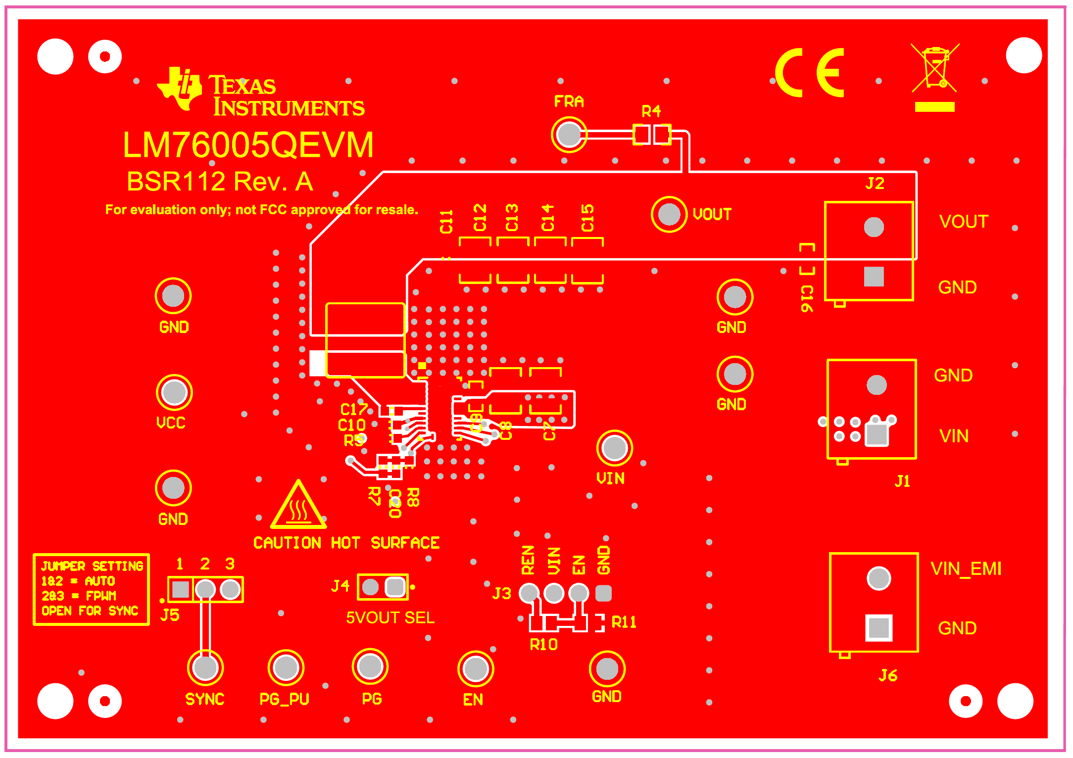 Figure 4-1 Top
Silkscreen Layer
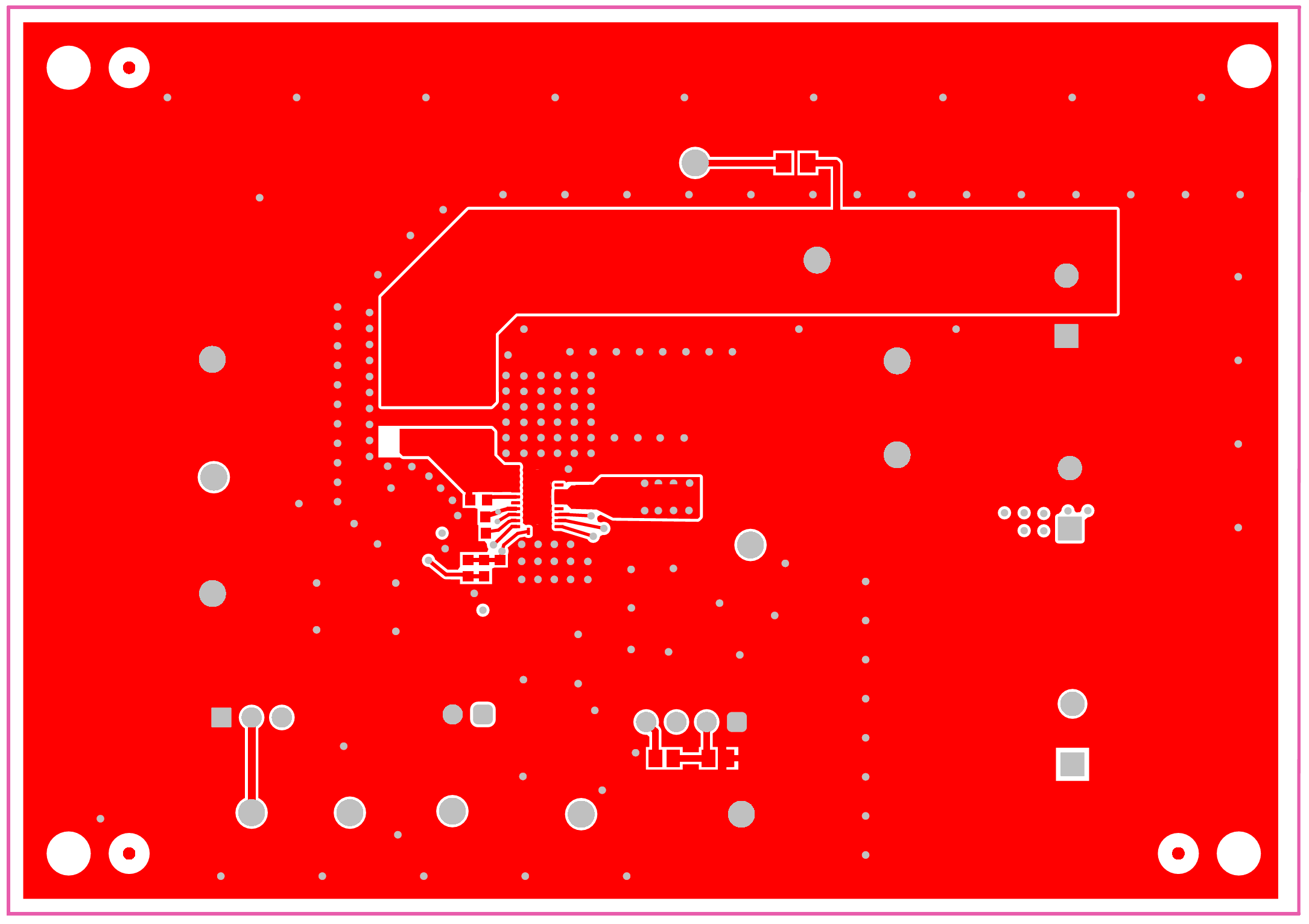 Figure 4-2 Top Layer
Routing
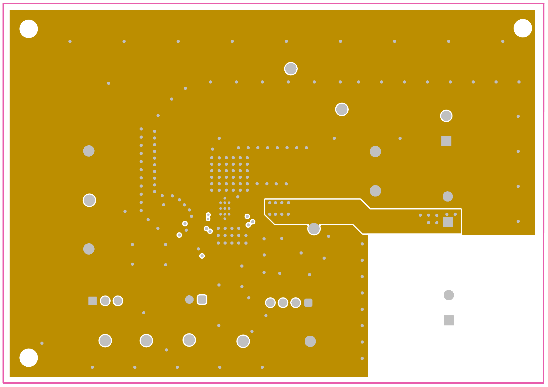 Figure 4-3 Mid Layer
1 Ground Plane
 Figure 4-4 Mid Layer
2 Routing
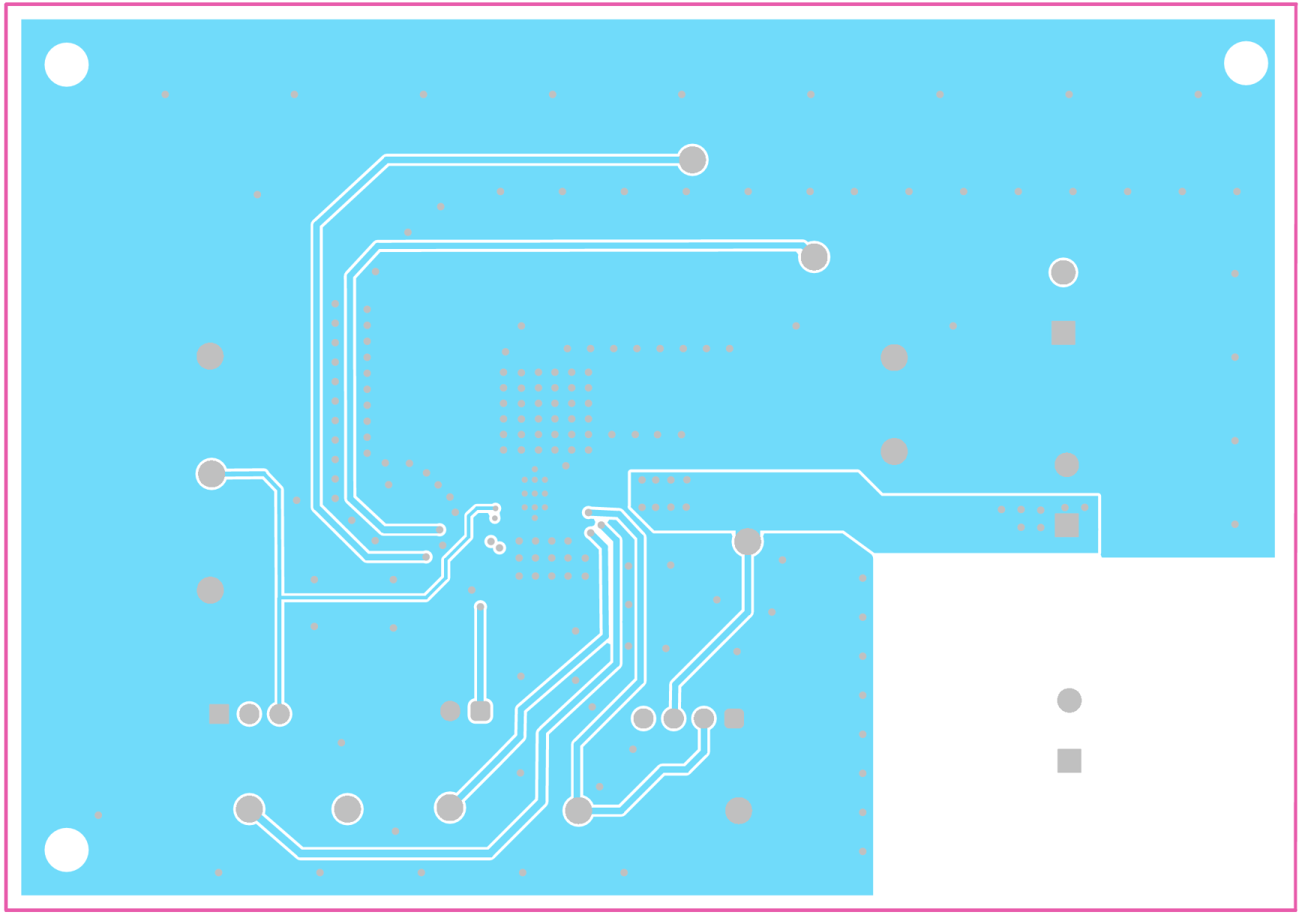 Figure 4-5 Bottom
Layer Routing
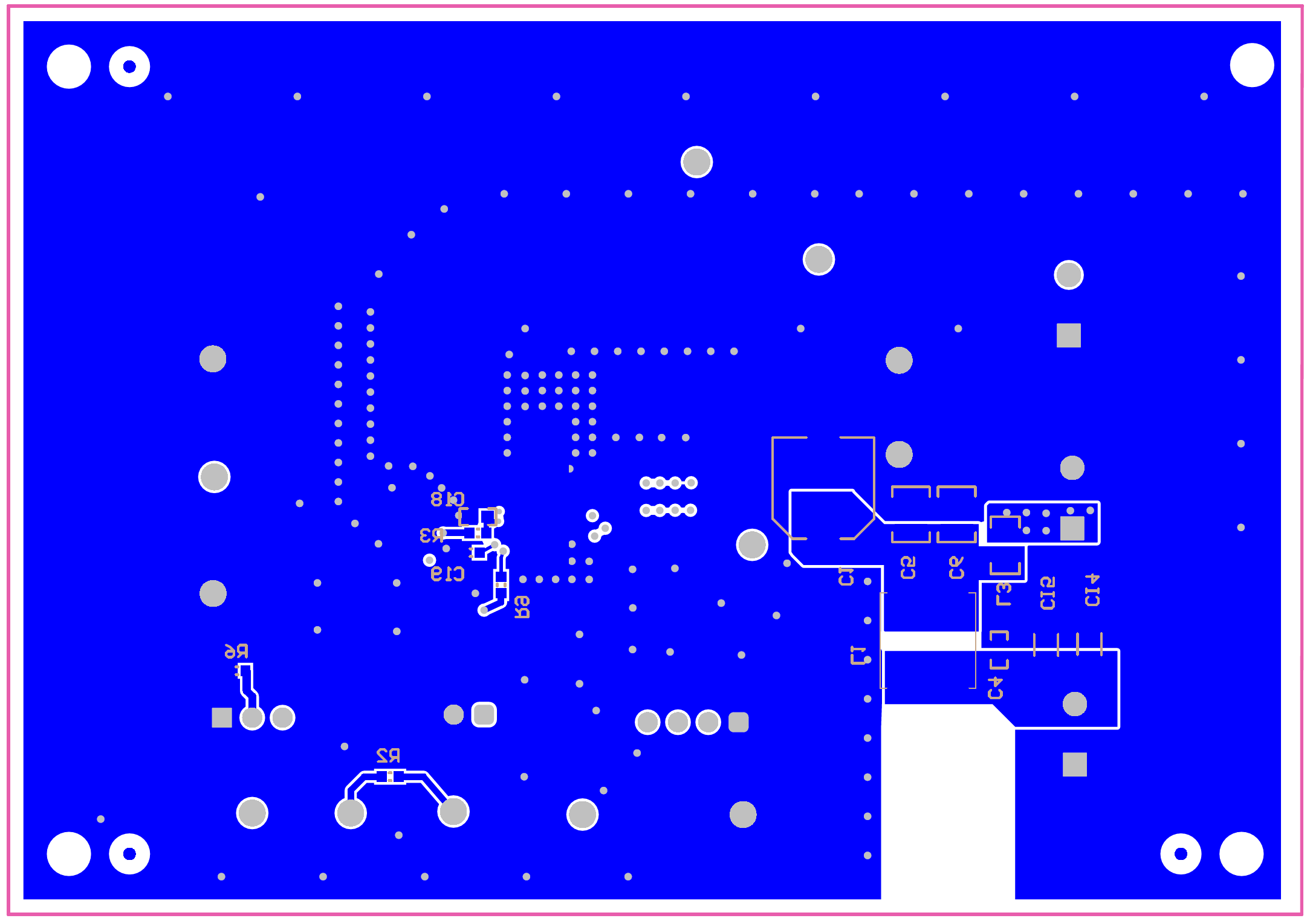 Figure 4-6 Bottom Layer Routing